
Eureka
For R&D, Eureka makes reading and utilizing patents & technical documents easy.
Eureka AIR
Designed for self-driven R&D workflows. Generate viable solutions, solve complex R&D challenges, empower your innovation with AI.

Eureka Materials
Designed for material experts only. Revolutionize your material R&D, from search, analyze, to developing new materials.

TechResearch
Generate reliable direction feasibility study reports for your R&D in just a few steps.

TechSeek
Discover and master advanced knowledge NOW. Basics, ideas, possibilities, all at once.

TechMind
As an expert in R&D Theories, TechMind can generates customized viable solutions instantly.

TechRisk
Analyze your overall solution with one click, know your potential R&D risks in advance.

TechMonitor
Get weekly tech updates, stay abreast of the latest tech innovations and key insights.
Die molding for flip chip molded matrix array package using UV curable tape
- Summary
- Abstract
- Description
- Claims
- Application Information
AI Technical Summary
Problems solved by technology
Method used
Image

Examples
Example
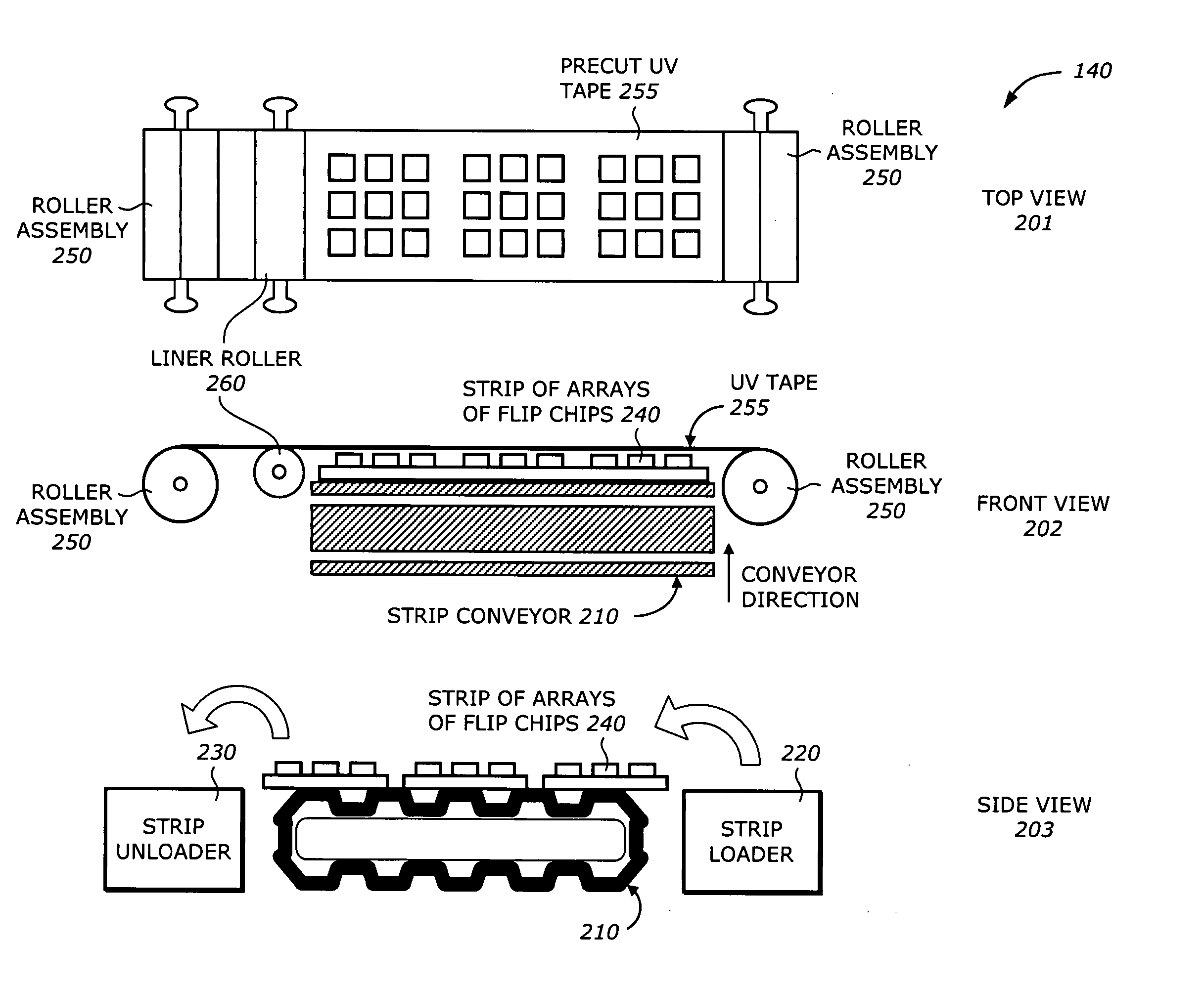
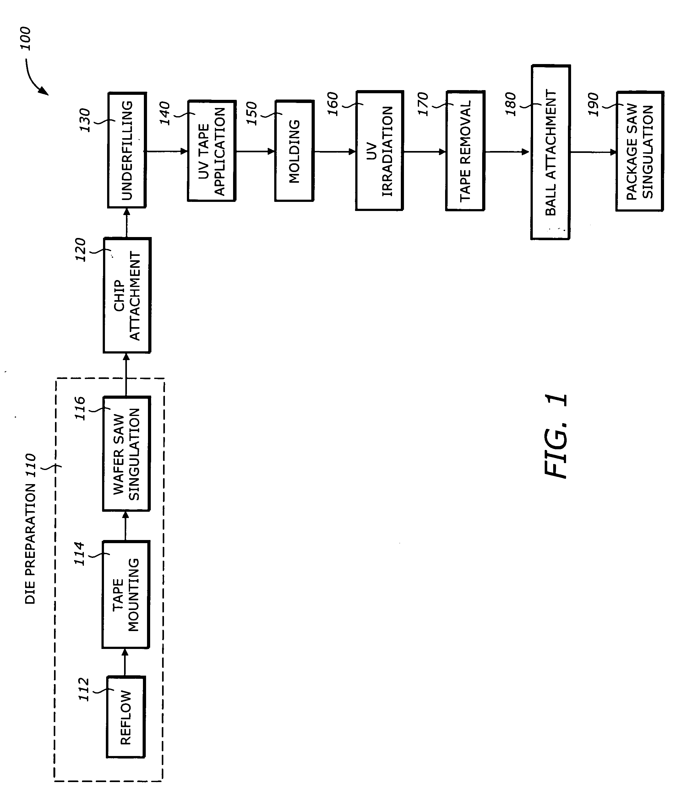
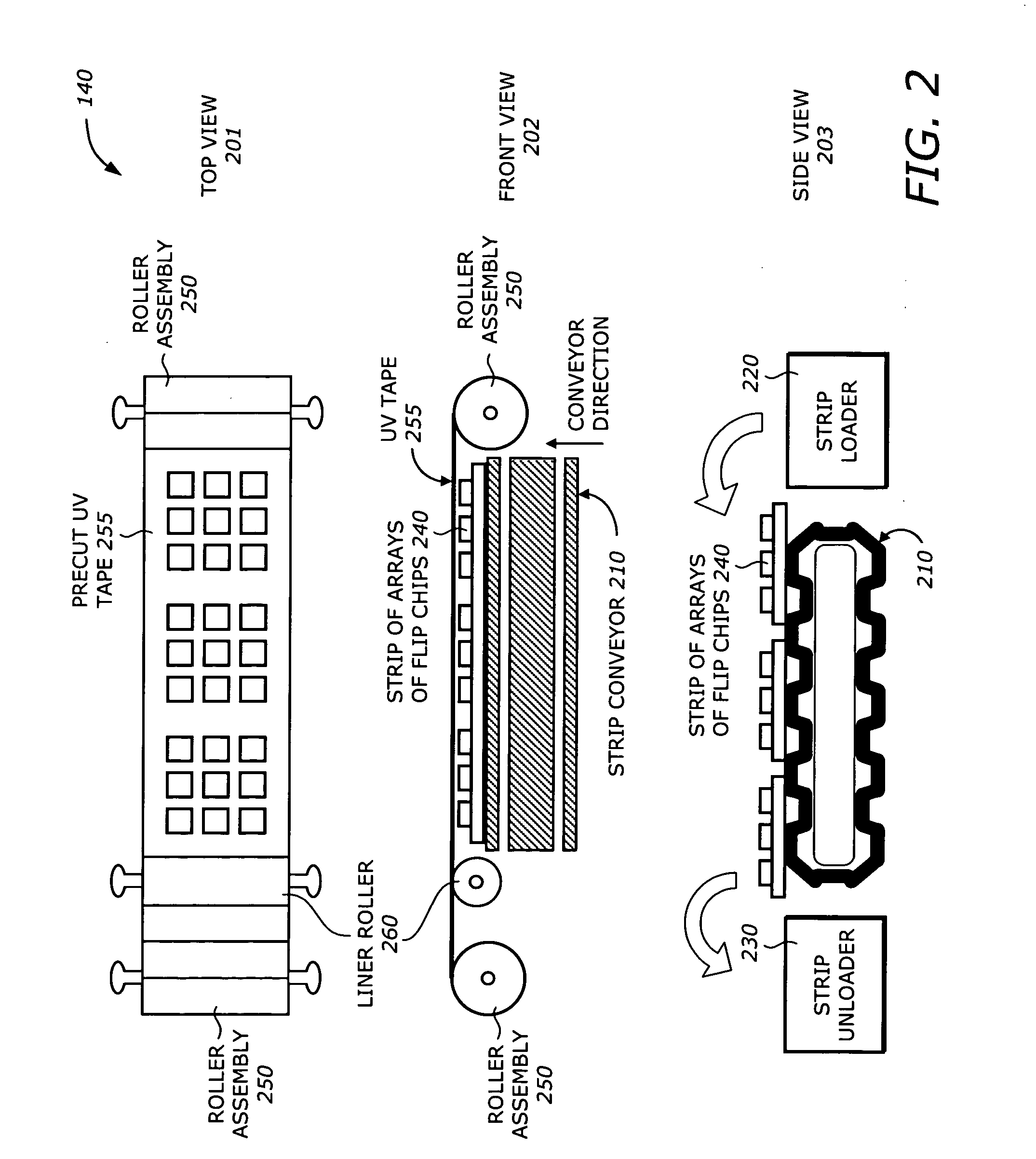
[0015] An embodiment of the present invention is a technique to package flip chip array. An ultraviolet (UV) curable tape is laminated on die backside of a strip of arrays of flip chips. The UV curable tape has an adhesive strength. The strip of flip chip array is molded with a mold film. The molded strip of flip chip array is irradiated using UV radiation. In another embodiment, a double functional tape is mounted to backside of a wafer during the die preparation phase. The double functional tape includes a binding tape and an ultraviolet (UV) curable tape having an adhesive strength. The mounted wafer is then saw singulated into die. Subsequently, the die is attached to the substrate strip in array form. During the molding phase, the strip of arrays is molded with a mold film. The molded strip of arrays is irradiated using UV radiation.
[0016] In the following description, numerous specific details are set forth. However, it is understood that embodiments of the invention may be p...
PUM
| Property | Measurement | Unit |
|---|---|---|
| Adhesion strength | aaaaa | aaaaa |
Abstract
Description
Claims
Application Information
 - R&D Engineer
- R&D Manager
- IP Professional
- Industry Leading Data Capabilities
- Powerful AI technology
- Patent DNA Extraction
Browse by: Latest US Patents, China's latest patents, Technical Efficacy Thesaurus, Application Domain, Technology Topic, Popular Technical Reports.
© 2024 PatSnap. All rights reserved.Legal|Privacy policy|Modern Slavery Act Transparency Statement|Sitemap|About US| Contact US: help@patsnap.com