Semiconductor nanoparticle and method for producing same

a technology of semiconductors and nanoparticles, applied in the field of semiconductor nanoparticles, can solve the problems of inconvenient handling of semiconductor nanoparticles, and achieve the effect of facilitating handling

Inactive Publication Date: 2005-07-07
HITACHI LTD
View PDF5 Cites 38 Cited by
  • Summary
  • Abstract
  • Description
  • Claims
  • Application Information

AI Technical Summary

Benefits of technology

[0029] A major feature of the semiconductor nanoparticle of the invention on which the aforementioned electron-releasing groups are arranged is that it is water-soluble, such that it can be handled with ease in various applications.
[0030] In a third aspect, the invention provides

Problems solved by technology

For these reasons, the semiconductor nanoparticles have been gaining attention in recent years, and the solving of the aforementioned problems has been an issue among researchers.
Nevertheless, the result

Method used


Image

  • Semiconductor nanoparticle and method for producing same
  • Semiconductor nanoparticle and method for producing same
  • Semiconductor nanoparticle and method for producing same

Examples


example 1

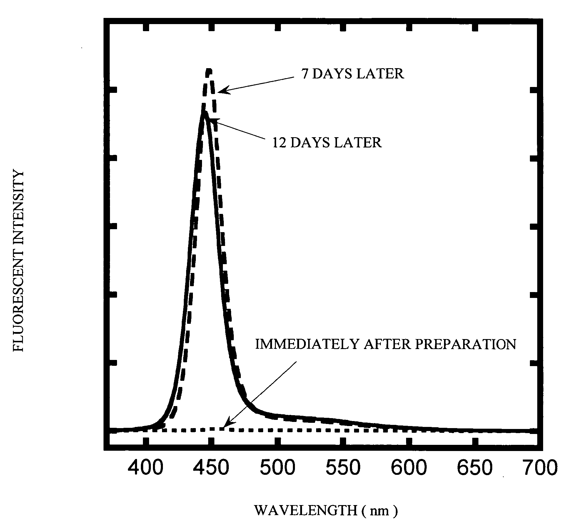
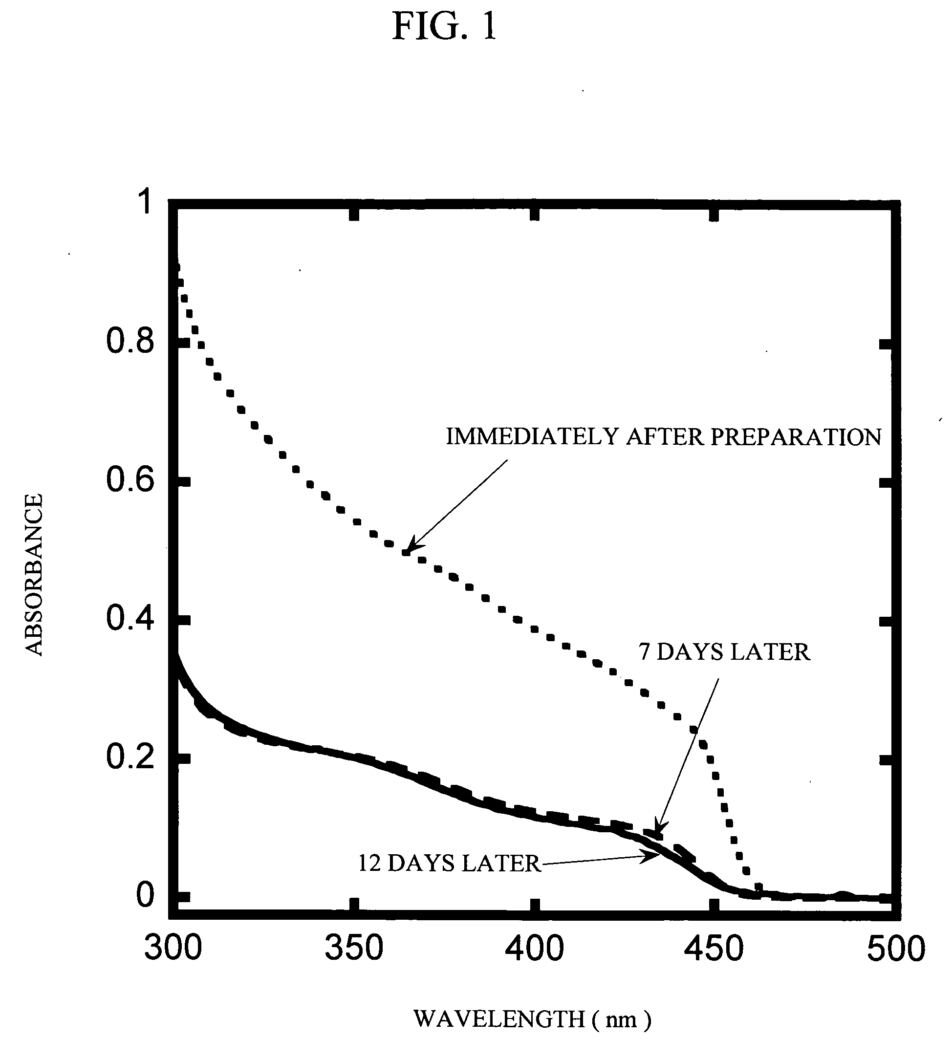
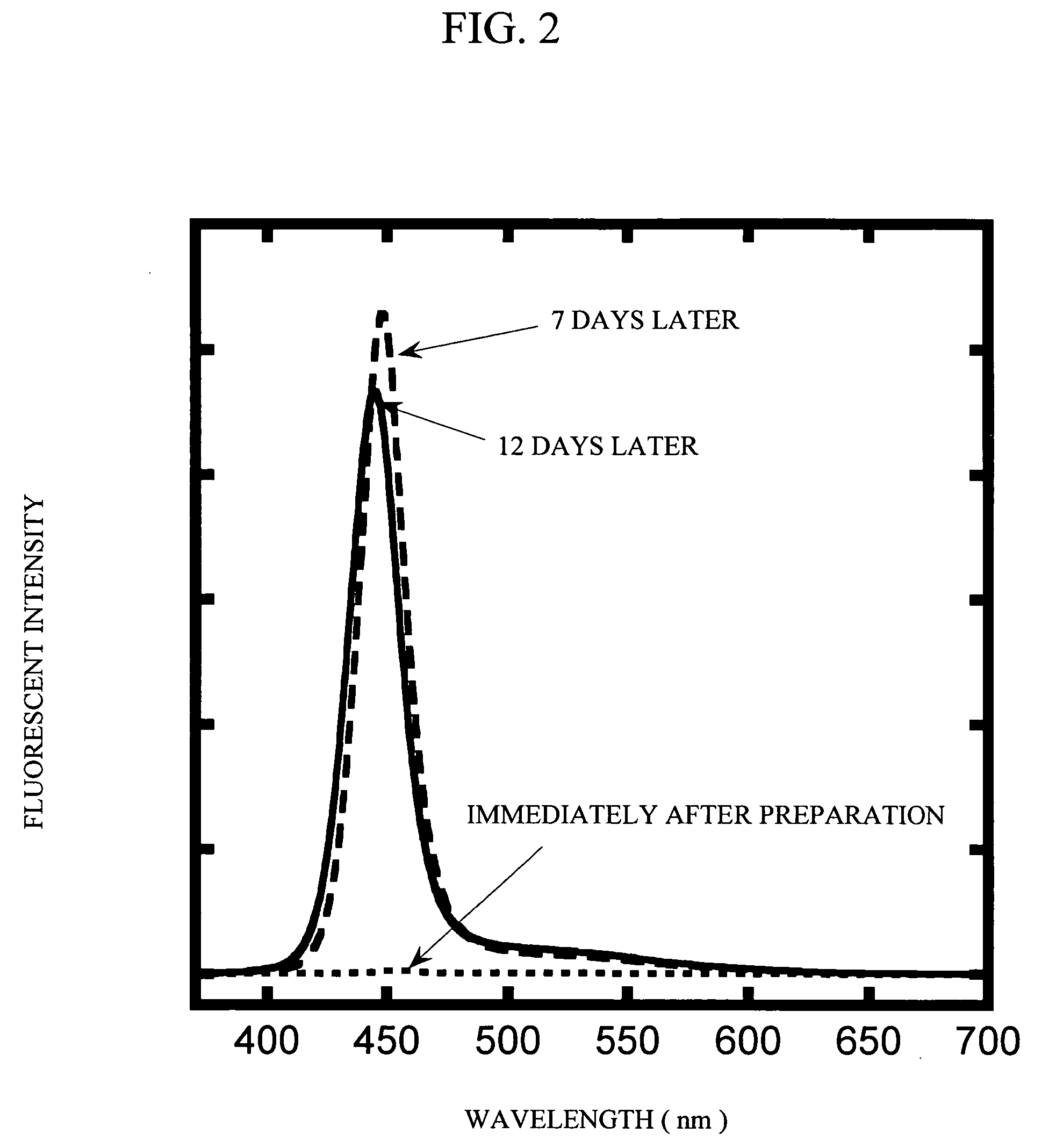
[0061] An aqueous solution of the purified and thiol-modified nanoparticles was diluted to an absorbance of 0.5 using an aqueous solution of 0.1 M NH3-HCl of pH 11. The solution was allowed to stand for several days to several weeks, thereby obtaining a semiconductor nanoparticle solution with high-emission properties. The resultant solution was optically transparent yellow and had superior emission properties. Temporal changes in the absorbance in accordance with this preparation process are shown in FIG. 1, and temporal changes in the fluorescent intensity are shown in FIG. 2.

example 2

[0062] An aqueous solution of the purified and thiol-modified nanoparticles was diluted to an absorbance of 0.5 using an aqueous solution of 0.1 M dimethylamine-HCl of pH 11. The solution was allowed to stand for several days to several weeks, thereby obtaining a semiconductor nanoparticle solution with high-emission properties. The resultant solution was optically transparent yellow and had superior emission properties. Temporal changes in the absorbance in accordance with this preparation process are shown in FIG. 3, and temporal changes in the fluorescent intensity are shown in FIG. 4.

example 3

[0063] An aqueous solution of the purified and thiol-modified nanoparticles was diluted to an absorbance of 0.5 using an aqueous solution of 0.1 M tetramehylamine-HCl of pH 11. The solution was allowed to stand for several days to several weeks, thereby obtaining a semiconductor nanoparticle solution with high-emission properties. The resultant solution was optically transparent yellow and had superior emission properties. Temporal changes in the absorbance in accordance with this preparation process are shown in FIG. 5, and temporal changes in the fluorescent intensity are shown in FIG. 6.


PUM

PropertyMeasurementUnit
Solubility (mass)aaaaaaaaaa
Fluorescenceaaaaaaaaaa

Abstract

The invention provides a semiconductor nanoparticle comprising a semiconductor nanoparticle core on the surface of which electron-releasing groups are arranged, the semiconductor nanoparticle having a fluorescent property and water-solubility. The invention also provides a water-soluble semiconductor nanoparticle with an excellent fluorescent property that can be easily prepared by adding a surface-treating material for providing a semiconductor nanoparticle with one or more kinds of electron-releasing groups, and arranging the electron-releasing groups on the surface of the semiconductor nanoparticle core.

Description

FIELD OF THE INVENTION [0001] The present invention relates to a semiconductor nanoparticle and a process of manufacturing the same. In particular, the invention relates to a stable and water-soluble semiconductor nanoparticle and a process of manufacturing the same. The invention also relates to a fluorescent reagent and an optical device comprising the semiconductor nanoparticle. BACKGROUND ART [0002] Semiconductor nanoparticles with a particle size of less than 10 nm lie in a transition region between bulk semiconductor crystals and molecules. They exhibit physicochemical properties that are different from those of both bulk semiconductor crystals and molecules. In this region, the energy gap of the semiconductor nanoparticles increases with decreasing particle size, due to the emergence of the quantum size effect. This is further accompanied by the removal of the energy band degeneracy that is observed in bulk semiconductors, so that the orbits become discrete, with the lower en...

Claims


Application Information

Patent Timeline
IPC IPC(8): B82B1/00B82B3/00C09C1/12C09C3/08C09K11/02C09K11/08C09K11/54C09K11/55C09K11/56C09K11/59C09K11/64C09K11/66C09K11/67C09K11/68C09K11/70C09K11/74C09K11/88
CPCB82Y30/00Y10S977/83C01P2004/64C09C1/12C09C3/08C09K11/0883C09K11/0894C09K11/54C09K11/56C09K11/565C09K11/59C09K11/66C09K11/68C09K11/88C09K11/883Y10T428/2991Y10S977/773Y10S977/783Y10S977/904Y10S977/834Y10S977/949Y10S977/813C01P2002/84
Inventor SATO, KEIICHIKUWABATA, SUSUMU
Owner HITACHI LTD
Why Eureka
Try Eureka