

Semiconductor integrated circuit device
a technology of integrated circuits and semiconductors, applied in the direction of power consumption reduction, pulse techniques, instruments, etc., can solve the problems of difficult to suppress a process variation with sufficient accuracy, increase the ratio of a leak current to a power consumption, and reduce the threshold. , to achieve the effect of saving power consumption, effective power consumption, and suppressing leak curren
- Summary
- Abstract
- Description
- Claims
- Application Information
AI Technical Summary
Benefits of technology
Problems solved by technology
Method used
Image

Examples
first embodiment
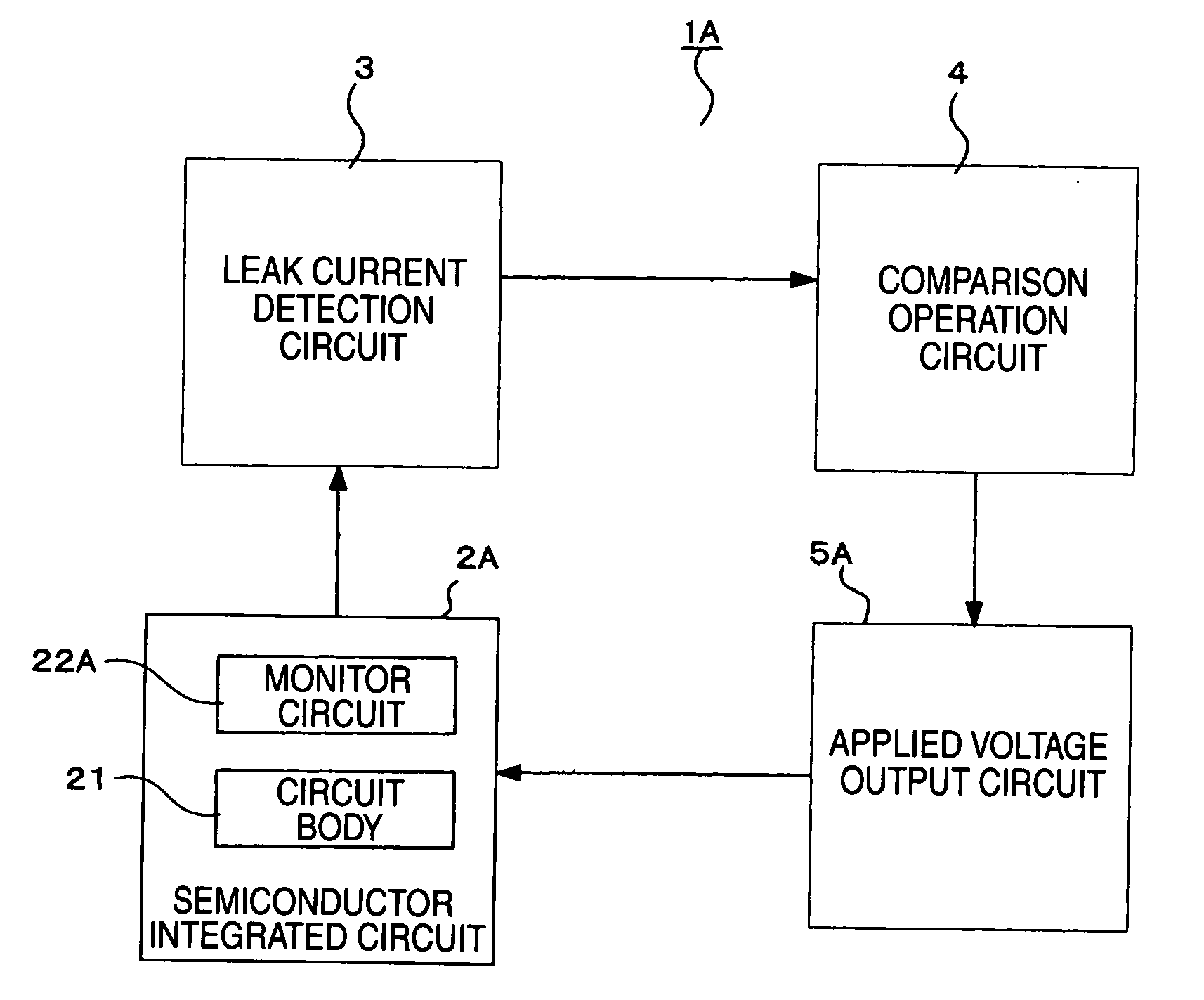
[0082]FIG. 1 is a block diagram showing the schematic configuration of a semiconductor integrated circuit device 1A according to a first embodiment of the invention. The semiconductor integrated circuit device 1A includes a semiconductor integrated circuit 2A, a leak current detection circuit 3, a comparison operation circuit 4 and an applied voltage output circuit 5A.
[0083] The semiconductor integrated circuit 2A has a circuit body 21 and a monitor circuit 22A. The circuit body 21 has a plurality of MOSFETs and performs predetermined functional operations as microprocessors, digital signal processors, etc. The monitor circuit 22A has MOSFETs formed in the same process specifications as the MOSFETs of the circuit body 21. Leak currents from the MOSFETs (hereinafter referred to as “monitor MOSFETs”) in the monitor circuit 22A are detected so that the source-substrate voltage or the like of the MOSFETs (hereinafter referred to as “functional MOSFETs”) of the circuit body 21 can be ad...
second embodiment
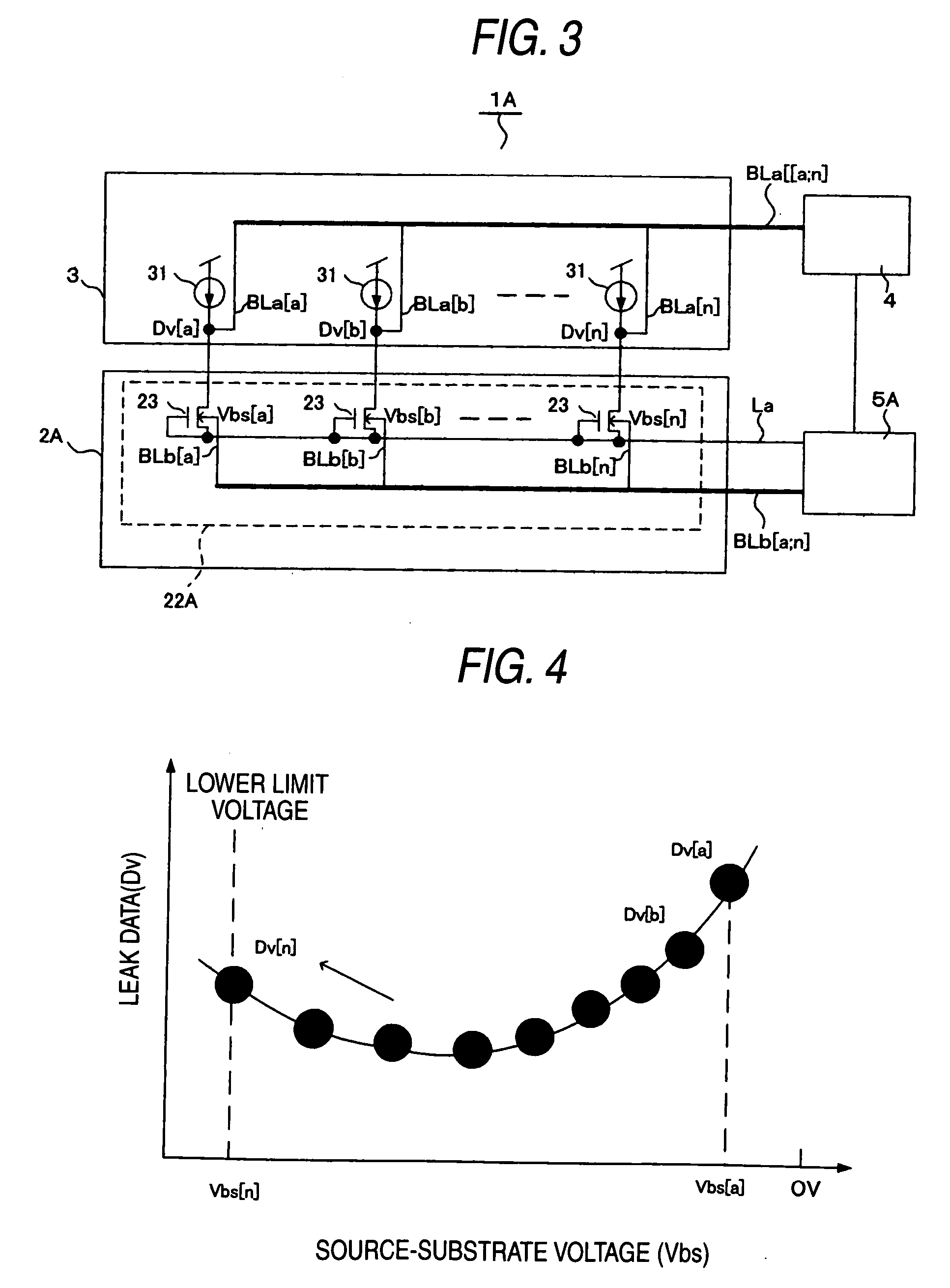
[0106] Next, a second embodiment will be described. Constituent members the same as those in the first embodiment are referenced correspondingly, and description thereof will be omitted. In this embodiment, a leak current is suppressed by adjusting a source-drain voltage.
[0107]FIG. 7 is a block diagram of a semiconductor integrated circuit device 1B according to this embodiment, showing the details of the configuration of a monitor circuit 22B in a semiconductor integrated circuit 2B and the leak current detection circuit 3. The monitor circuit 22B has a configuration similar to that of the monitor circuit 22A. However, gates and sources of a plurality of monitor NMOSFETs 23 are connected to each other, and connected to an applied voltage output circuit 5B through a source voltage bus BLc [a:n]. In addition, drains of the monitor NMOSFETs 23 are connected to current sources 31 respectively, and a leak data bus BLa [a:n] is connected to connection points between the drains and the c...
third embodiment
[0116] Next, a third embodiment will be described. Constituent members the same as those in the first and second embodiments are referenced correspondingly, and description thereof will be omitted. In the first and second embodiments, the leak current detection circuit 3 and the comparison operation circuit 4 are connected through the leak data bus BLa. On the other hand, in this embodiment, a leak current detection circuit 3 and a comparison operation circuit 4 are connected not through a bus but through a line, while leak data Dv of monitor NMOSFETs 23 can be sampled sequentially.
[0117]FIG. 10 is a block diagram of the comparison operation circuit 4 according to this embodiment, which has a data holding circuit 41 and a comparison circuit 42. Leak data Dv from the leak current detection circuit 3 are inputted to the data holding circuit 41 and the comparison circuit 42.
[0118] The data holding circuit 41 operates in response to a trigger signal so as to sample the leak data Dv an...
PUM
 Abstract
Description
Claims
Application Information