

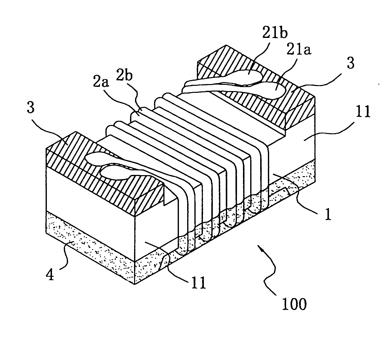
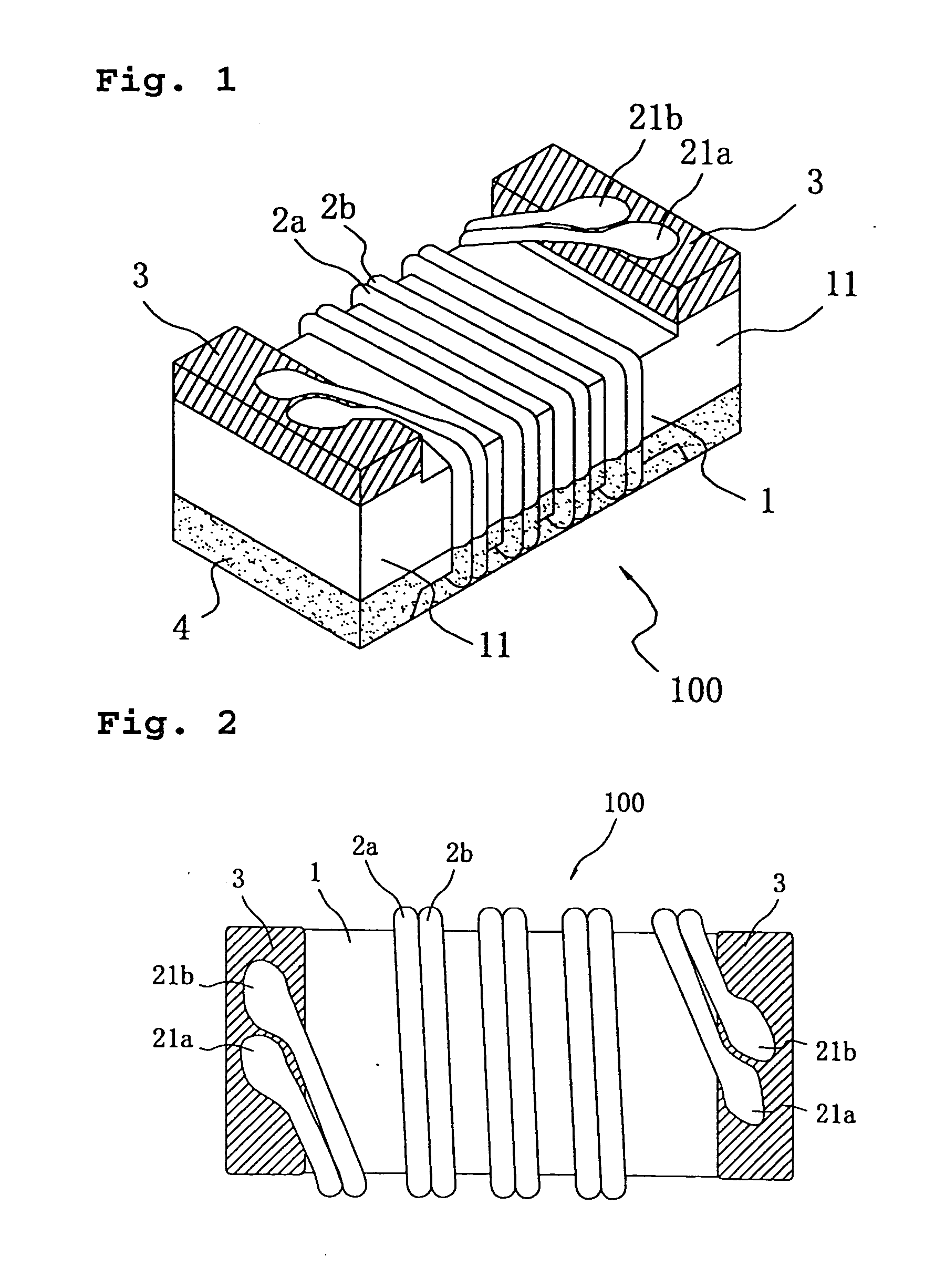
Wire-wound type chip coil and method of adjusting a characteristic thereof
a chip coil and wire-wound technology, applied in the field of wire-wound chip coils, can solve the problems of difficult process needed to adjust the matching between a circuit element and a transmission line, limited inductance to corresponding values, and limited inductance available to special values, and achieves the effect of simple structur
- Summary
- Abstract
- Description
- Claims
- Application Information
AI Technical Summary
Benefits of technology
Problems solved by technology
Method used
Image

Examples
first embodiment
[0050] In the table shown in FIG. 11, values of inductance obtained by winding two conductive wires with a diameter of about 50 μm regularly in a single layer around a 1005-size core are shown in a row denoted by “FIRST EMBODIMENT”. In this case, in contrast to the “CONVENTIONAL TECHNIQUE” in which 1.5 nH and 2.7 nH are obtained respectively for one-turn and two-turn coils of one conductive wire, use of two conductive wires results in reductions in inductance down to about 1.2 nH and about 2.4 nH for one-turn and two-turn coils respectively.
[0051] As described earlier, when a single conductive wire with a diameter of about 80 μm is wound one turn around a 1608-size core, resultant inductance is about 2.2 nH. Herein, if the single conductive wire is replaced with two conductive wires, the inductance decreases to about 1.8 nH. If the number of substantially parallel conductive wires is further increased, a further reduction in inductance is achieved. Thus, by properly selecting the nu...
second embodiment
[0056] In this wire-wound type chip coil according to the second preferred embodiment, the conductive wires 2a and 2b are wound around the main portion 12 of the core 1 such that the conductive wires 2a and 2b are spaced from each other and such that the distance between any adjacent wires becomes substantially equal. In the table shown in FIG. 11, in a row denoted by “SECOND EMBODIMENT”, shown are values of inductance obtained by winding two conductive wires with a diameter of about 50 μm around a 1005-size core such that the conductive wires are spaced from each other and such that the distance between any adjacent wires becomes substantially equal. As can be seen, an inductance of about 1.1 nH to about 1.3 nH is obtained by a one-turn coil of two wires, and inductance of about 1.8 nH to about 2.4 nH is obtained by a two-turn coil.
[0057] Thus, inductance of about 2.4 nH for a two-turn regularly-wound single-layer coil can be reduced to about 1.8 nH by expanding the space between t...
third embodiment
[0061] In this preferred embodiment, unlike the wire-wound type chip coil according to the second preferred embodiment, two conductive wires 2a and 2b are regularly wound in a single layer around the main portion 12 of the core, and the space between one of the two conductive wires at a certain turn and the other one of the two conductive wires at an adjacent turn is adjusted so as to obtain a desired value of inductance. In the table shown in FIG. 11, in a row denoted by “THIRD EMBODIMENT”, shown are values of inductance obtained by winding two conductive wires with a diameter of about 50 μm around a 1005-size core. As can be seen, inductance of about 2.0 nH to about 2.4 nH is obtained by a by a two-turn coil of two wires.
[0062]FIG. 9 shows the inductance as a function of the space between the two conductive wires, for a two-turn coil using conductive wires with a diameter of about 50 μm. Inductance of about 2.2 nH is obtained when the wire-to-wire space between adjacent turns is a...
PUM
| Property | Measurement | Unit |
|---|---|---|
| thickness | aaaaa | aaaaa |
| diameters | aaaaa | aaaaa |
| inductance | aaaaa | aaaaa |
Abstract
Description
Claims
Application Information