
Electro-optical device

a liquid crystal display and pixel region technology, applied in optics, identification means, instruments, etc., can solve problems such as inability to display, and achieve the effect of stable operation, improved shading effect, and advantageous stable operation of transistors

Inactive Publication Date: 2005-07-07
SEMICON ENERGY LAB CO LTD
View PDF87 Cites 1 Cited by
  • Summary
  • Abstract
  • Description
  • Claims
  • Application Information

AI Technical Summary

Benefits of technology

The invention is about a new configuration for a liquid crystal display (LCD) that solves the problem of unstable display and leakage of light caused by the electric field of adjacent electrodes. The invention includes a common electrode and a pixel electrode that overlap each other, creating an auxiliary capacitor. The common electrode is maintained at constant potential, and a film made of the same material as the source bus lines is provided on top of the gate bus lines to further improve stability. The use of a flat insulation layer formed by spin coating or the like can also improve uniformity of the electric field applied to liquid crystal molecules. The transparent conductive film used in the invention includes materials such as ITO, SnO2, and materials mainly composed of those materials.

Problems solved by technology

In practice, however, this results in unstable display because signals on bus lines affect pixel electrodes.

Method used


Image

  • Electro-optical device
  • Electro-optical device
  • Electro-optical device

Examples


first embodiment

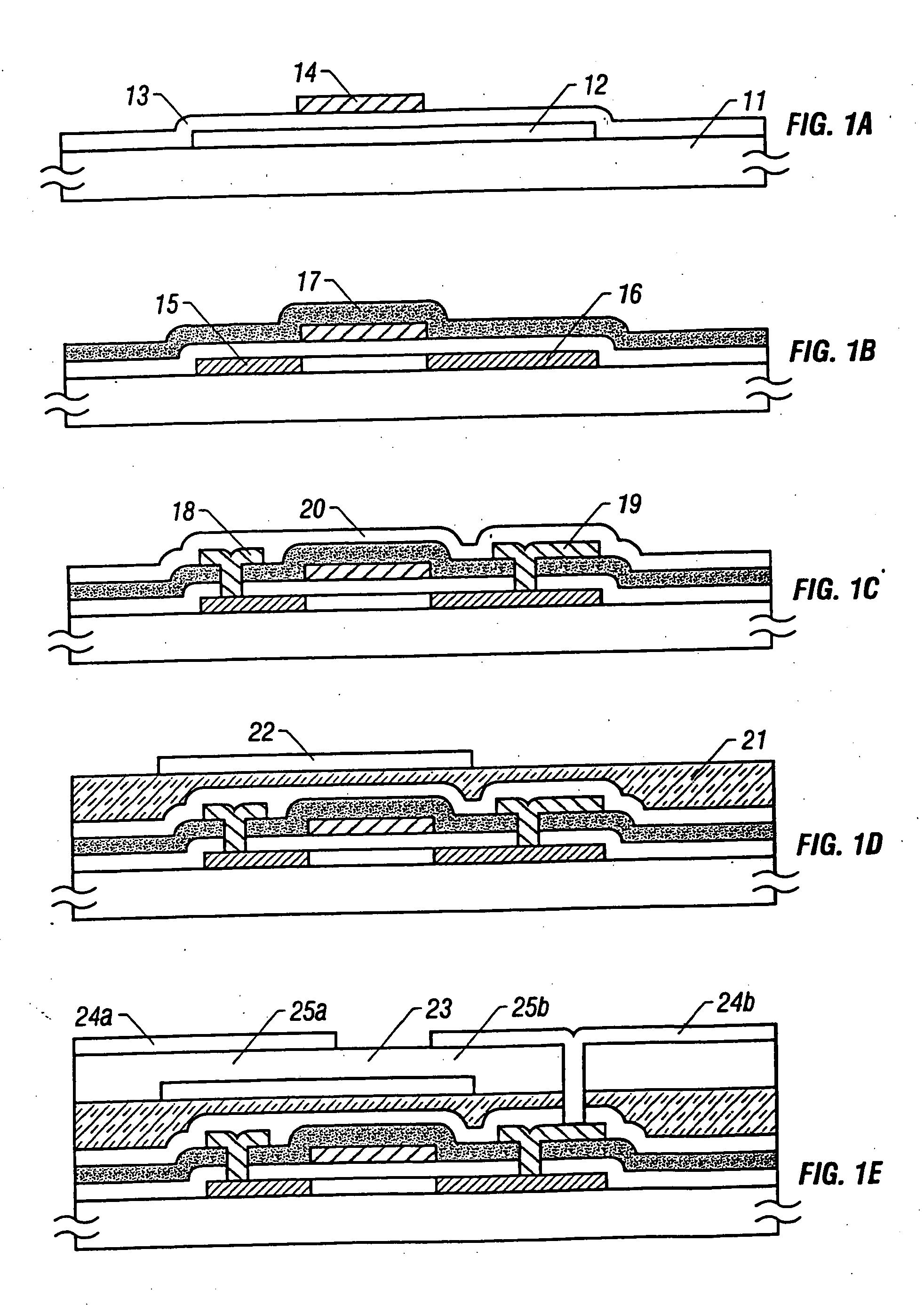
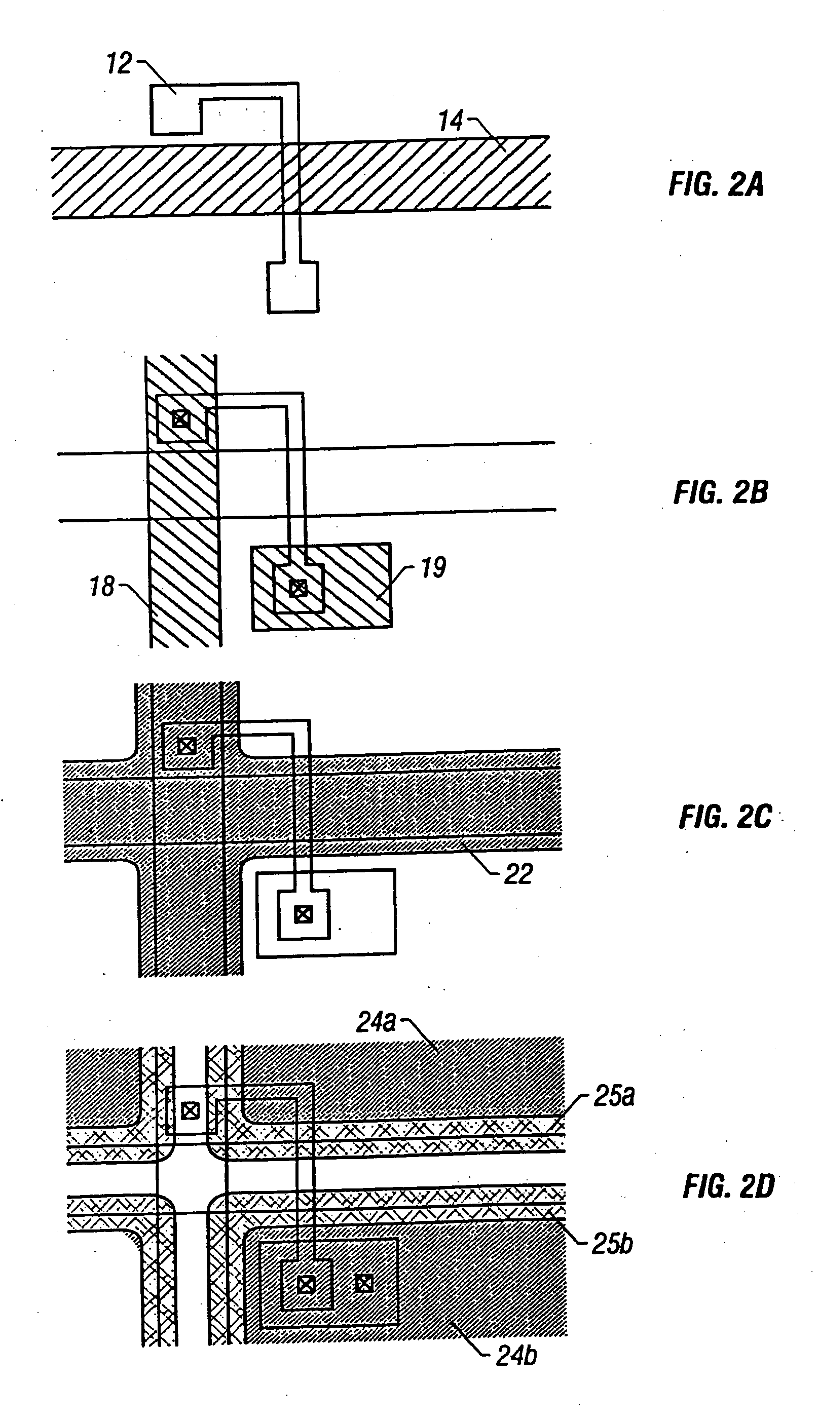
[0029] the present invention will now be described. FIGS. 1A through 1E and FIGS. 2A through 2D show a configuration of a pixel of an active matrix type liquid crystal display which employs the invention disclosed in this specification. FIGS. 1A through 1E are schematic sectional views showing fabrication steps according to the present embodiment, and FIGS. 2A through 2D show the configuration of each of a bus line, a common electrode, pixel electrodes, a semiconductor layer, and the like according to the present embodiment. The reference numbers in FIGS. 2A through. 2D are in correspondence with those in FIGS. 1A through 1E. FIGS. 1A through 1E are conceptual views and are not exactly identical to FIGS. 2A through 2D in configuration.

[0030] Further, FIGS. 1A through 1E and FIGS. 2A though 2D show a configuration of only a substrate on which a thin film transistor is provided. In practice, there is provided another substrate opposite thereto (opposite substrate), and liquid crystal ...

second embodiment

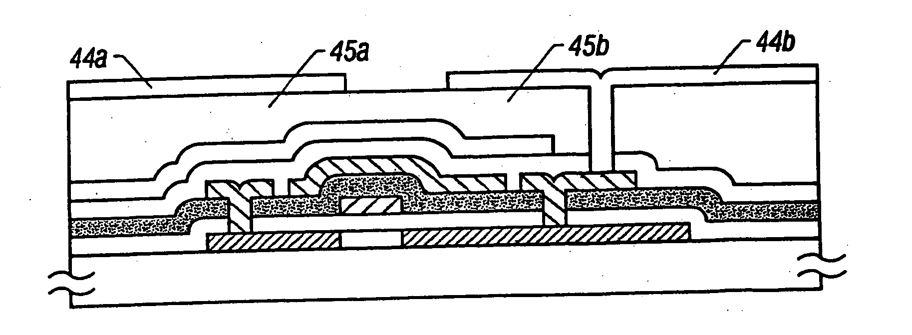
[0045] the present invention will now be described. FIGS. 3A through 3E and FIGS. 4A through 4D show a configuration of a pixel of an active matrix type liquid crystal display which employs the invention disclosed in this specification. FIGS. 3A through 3E are schematic sectional views showing fabrication steps according to the present embodiment, and FIGS. 4A through 4D show the configuration of each of a bus line, a common electrode, pixel electrodes, a semiconductor layer, and the like according to the present embodiment. The reference numbers in FIGS. 4A through 4D are in correspondence with those in FIGS. 3A through 3E. FIGS. 3A through 3E are conceptual views and are not exactly identical to FIGS. 4A through 4D in configuration.

[0046] As shown in FIG. 3A, a semiconductor layer lactive layer) 32 of a transistor is provided on a glass substrate 31 having an underlying silicon oxide film (not shown). A gate insulation film 33 is formed so as to cover the active layer 32. A gate b...


PUM

PropertyMeasurementUnit
insulatingaaaaaaaaaa
leak currentaaaaaaaaaa
electrical chargeaaaaaaaaaa

Abstract

An auxiliary capacitor for a pixel of an active matrix type liquid crystal display is provided without decreasing the aperture ratio. A transparent conductive film for a common electrode is formed under a pixel electrode constituted by a transparent conductive film with an insulation film provided therebetween. Further, the transparent conductive film for the common electrode is maintained at fixed potential, formed so as to cover a gate bus line and a source bus line, and configured such that signals on each bus line are not applied to the pixel electrode. The pixel electrode is disposed so that all edges thereof overlap the gate bus line and source bus line. As a result, each of the bus lines serves as a black matrix. Further, the pixel electrode overlaps the transparent conductive film for the common electrode to form a storage capacitor.

Description

BACKGROUND OF THE INVENTION [0001] 1. Field of the Invention [0002] The invention disclosed in this specification relates to a configuration of a pixel region of an active matrix type liquid crystal display and, more particularly, to a configuration of an auxiliary capacitor connected to a pixel electrode in parallel and a configuration of a black matrix for preventing leakage of light at boundaries between adjacent pixels. [0003] 2. Description of Related Art [0004] Liquid crystal displays having an active matrix circuit are known. They have a configuration including a plurality of source bus lines for transmitting image data, a plurality of gate bus lines for transmitting switching signals in an intersecting relationship therewith, and a plurality of pixels provided at those intersections. Normally, transistors (specifically thin film transistors) are used as switching elements. [0005] A pixel includes not only a transistor for switching but also a pixel electrode and has a struct...

Claims


Application Information

Patent Timeline
Patent Type & Authority Applications(United States)
IPC IPC(8): G02B5/00G02F1/1343G02F1/136G02F1/1362G02F1/1368G09F9/00H01L29/786
CPCG02F1/136209G02F1/136213G02F2201/40G02F1/136286G02F2201/121G02F1/136227
Inventor ZHANG, HONGYONGYAMAGUCHI, NAOAKITAKEMURA, YASUHIKO
Owner SEMICON ENERGY LAB CO LTD
Learn More