Transistor with nanocrystalline silicon gate structure

a transistor and nanocrystalline silicon technology, applied in the field of floating gate memory cells, can solve problems such as memory defects

Inactive Publication Date: 2005-07-07
MICRON TECH INC
View PDF34 Cites 33 Cited by
  • Summary
  • Abstract
  • Description
  • Claims
  • Application Information

AI Technical Summary

Problems solved by technology

A memory designed to use a tunnel-tunnel process typically has a gate oxide thickness of about 15-20 Å which can be degraded over time resulting in a defective memory.

Method used


Image

  • Transistor with nanocrystalline silicon gate structure
  • Transistor with nanocrystalline silicon gate structure
  • Transistor with nanocrystalline silicon gate structure

Examples


Embodiment Construction

[0018] In the following detailed description of the preferred embodiments, reference is made to the accompanying drawings which form a part hereof, and in which is shown by way of illustration specific preferred embodiments in which the inventions may be practiced. These embodiments are described in sufficient detail to enable those skilled in the art to practice the invention, and it is to be understood that other embodiments may be utilized and that logical, mechanical and electrical changes may be made without departing from the spirit and scope of the present inventions. The following detailed description is, therefore, not to be taken in a limiting sense, and the scope of the present inventions is defined only by the appended claims.

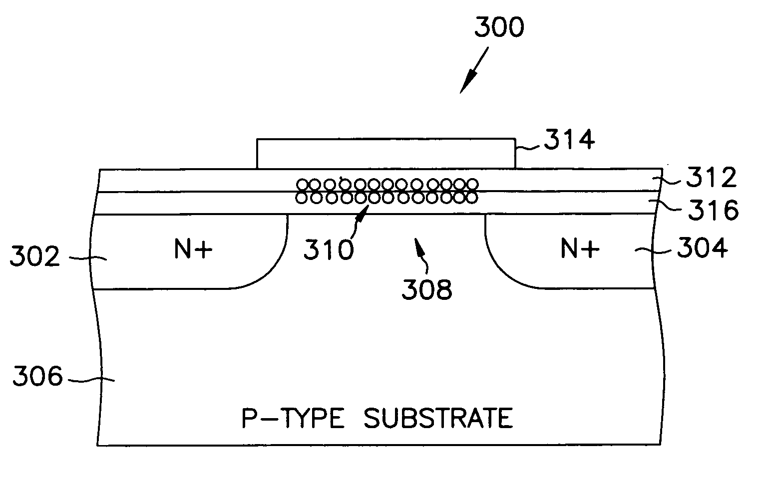
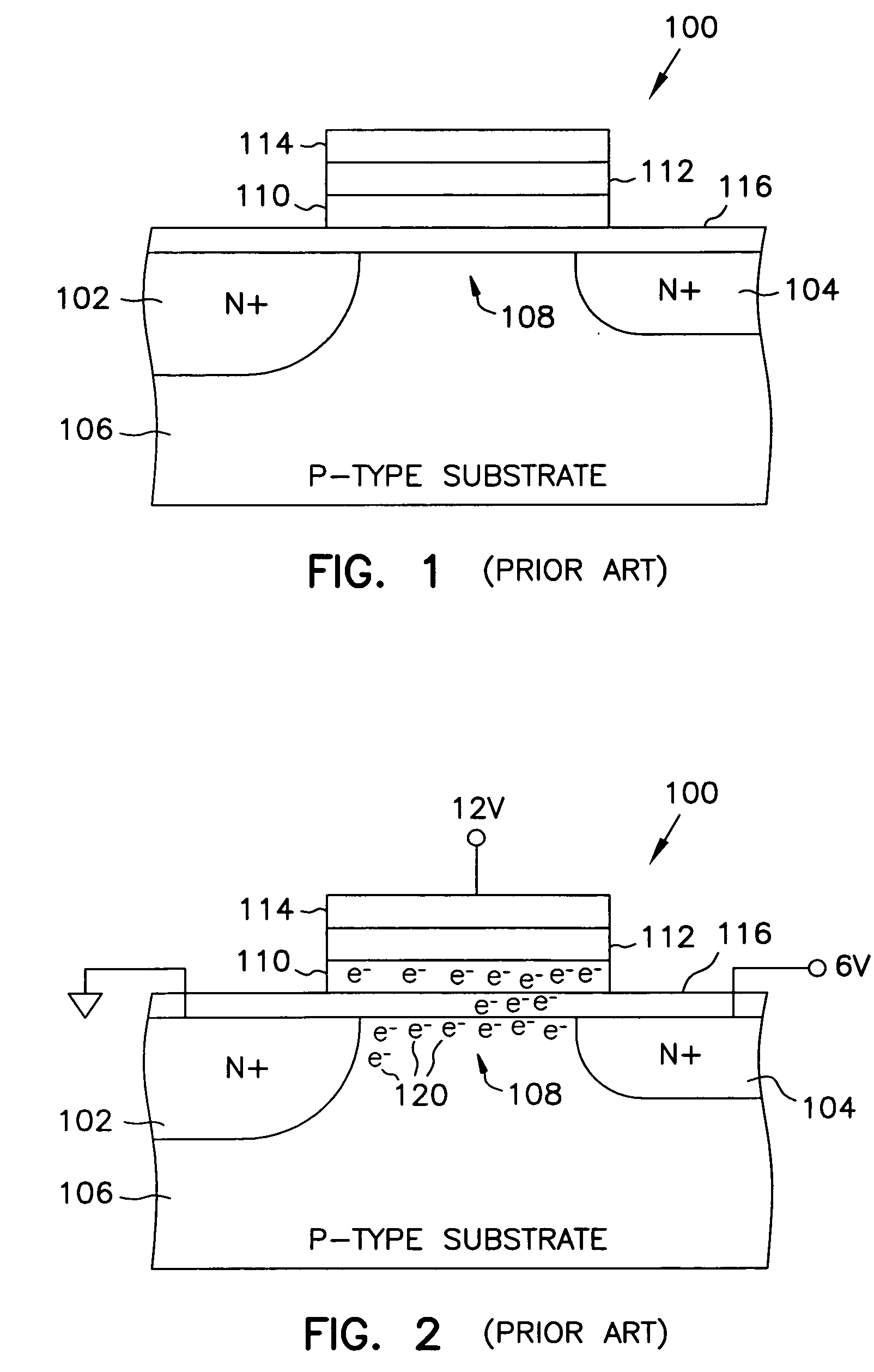
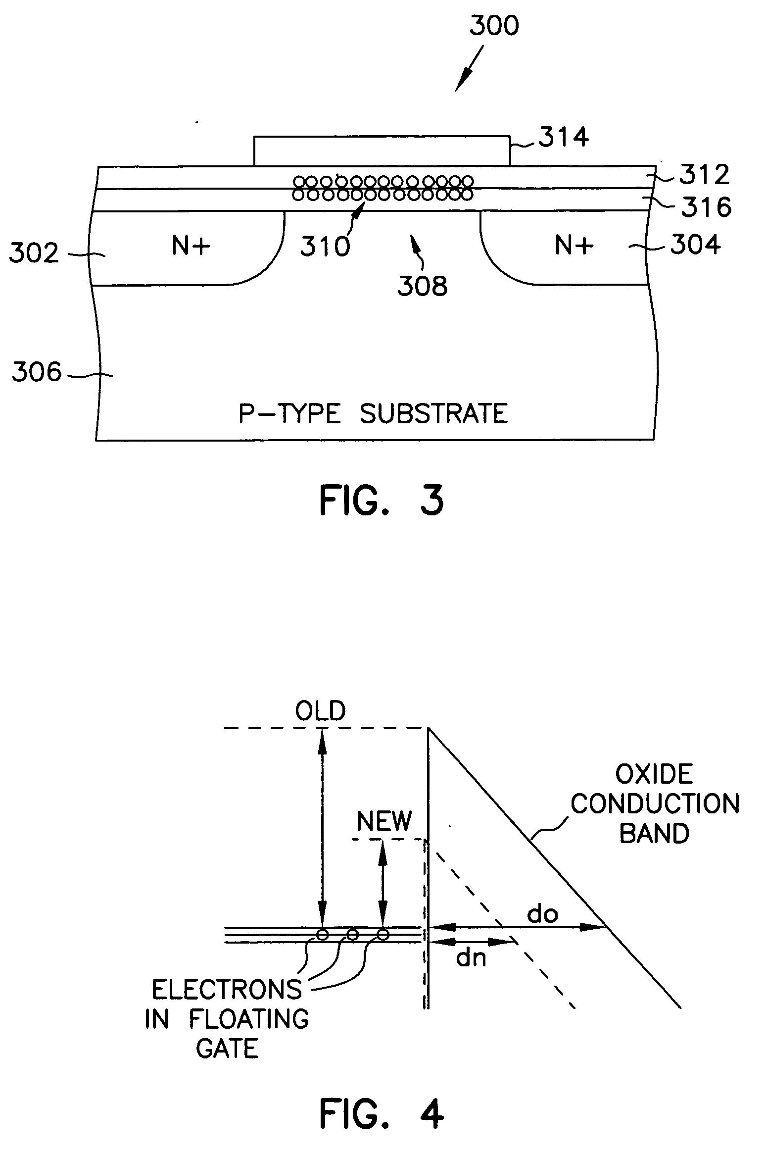
[0019]FIG. 1 is a cross-sectional view of a typical memory cell, such as a used in a flash memory. Memory cell 100 comprises a region of a source 102 and a region of a drain 104. Source 102 and drain 104 are constructed from an N+ type of high impu...


PUM


Abstract

A memory is described which has memory cells that store data using hot electron injection. The data is erased through electron tunneling. The memory cells are described as floating gate transistors wherein the floating gate is fabricated using a conductive layer of nanocrystalline silicon particles. Each nanocrystalline silicon particle has a diameter of about 10 Å to 100 Å. The nanocrystalline silicon particles are in contact such that a charge stored on the floating gate is shared between the particles. The floating gate has a reduced electron affinity to allow for data erase operations using lower voltages.

Description

CROSS-REFERENCE TO RELATED APPLICATION(S) [0001] This patent application is a continuation of U.S. patent application Ser. No. 10 / 453,324, filed Jun. 3, 2003, which is a continuation of U.S. patent application Ser. No. 10 / 176,425, now U.S. Pat. No. 6,574,144, which is a division of U.S. patent application Ser. No. 09 / 145,722, filed on Sep. 2, 1998, now U.S. Pat. No. 6,407,424, which is a continuation of U.S. patent application Ser. No. 08 / 790,500, filed on Jan. 29, 1997, now U.S. Pat. No. 5,852,306, the specifications of which are hereby incorporated by reference.TECHNICAL FIELD OF THE INVENTION [0002] The present invention relates generally to memory circuits and in particular the present invention relates to floating gate memory cells. BACKGROUND OF THE INVENTION [0003] Non-volatile memory such as electrically programmable read-only memory (EPROM) and electrically-erasable programmable read-only memory (EEPROM) are extensively used for storing data in computer systems. EPROM and E...

Claims


Application Information

Patent Timeline
Patent Type & Authority Applications(United States)
IPC IPC(8): H01L29/423H01L29/788
CPCH01L29/42332H01L29/7881Y10S977/763Y10S438/962Y10S977/723H01L29/7885
Inventor FORBES, LEONARD
Owner MICRON TECH INC
Why Eureka
Try Eureka