Optical burst switching node with internal speedup

a technology of optical burst switching and internal speedup, which is applied in the field of optical communication, can solve the problems of ineffective wavelength routing technology, inability to support wavelength packet switching effectively, and inability to achieve effective wavelength routing technology, etc., and achieves the effect of improving the buffering efficiency of fdl, increasing the internal bandwidth of obs nodes, and increasing the internal speed of nodes

Inactive Publication Date: 2005-07-14
UNIV OF ELECTRONICS SCI & TECH OF CHINA
View PDF14 Cites 13 Cited by
  • Summary
  • Abstract
  • Description
  • Claims
  • Application Information

AI Technical Summary

Benefits of technology

[0025] In summary, the present invention has the following characteristics: (1) by arranging multiple switching planes, the internal bandwidth of the OBS node is increased so as to achieve the internal speed-up of the node. As th

Problems solved by technology

But the two technologies have respective drawbacks.
On one side, the exponential growth of the network traffic focuses the interests of future networks on how to support packet traffic or service optimally, which the wavelength routing technology cannot support effectively.
On the other side, optical packet switching still faces many technical challenges in its implementation, such as lack of efficient optical logic devices, immaturity of optical buffer and difficulty in optical domain synchronization.
When performing optical switching at core nodes, there exists contention, when several bursts contend for the same wavelength of the same out

Method used


Image

  • Optical burst switching node with internal speedup
  • Optical burst switching node with internal speedup
  • Optical burst switching node with internal speedup

Examples


Embodiment Construction

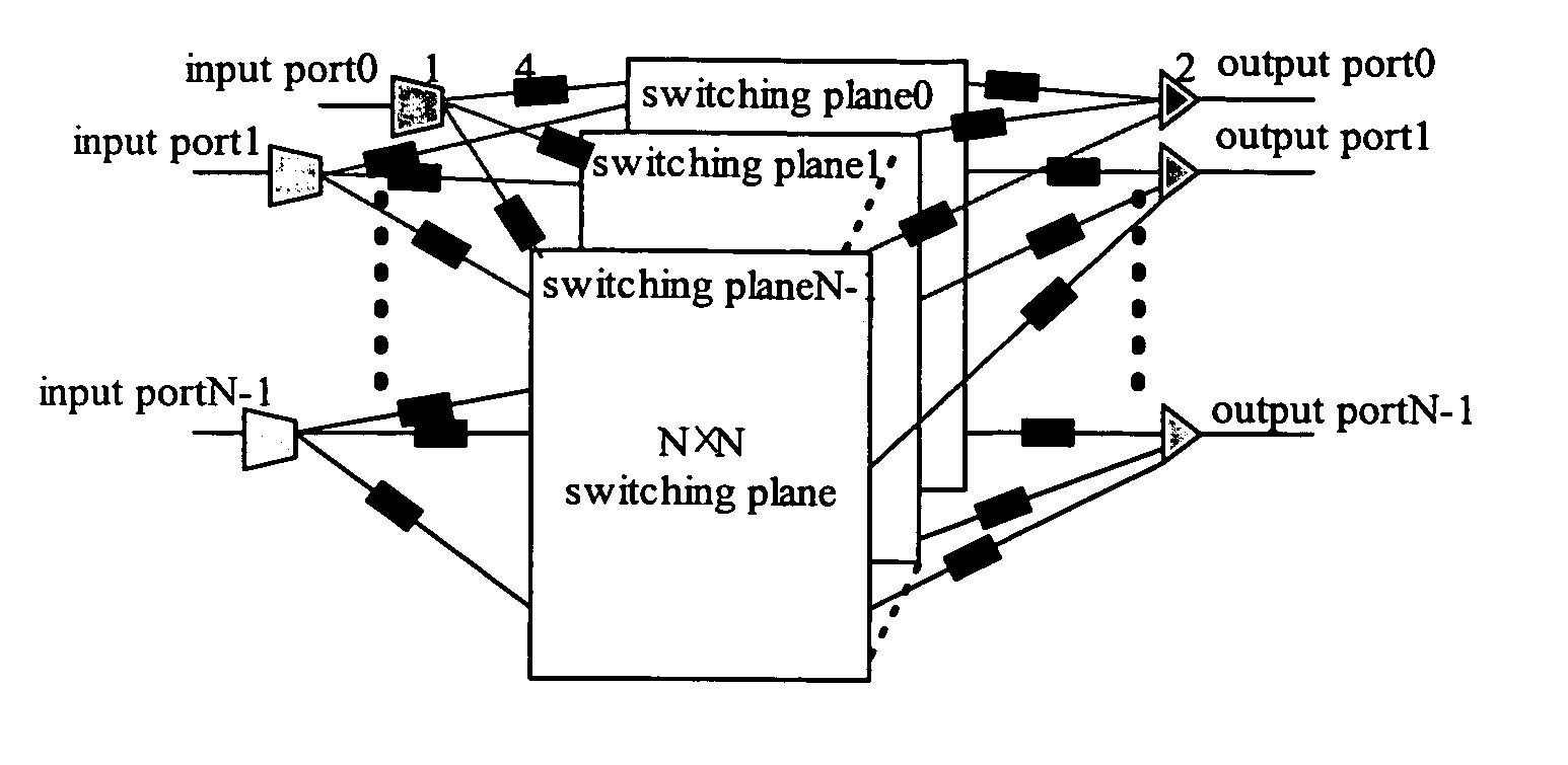
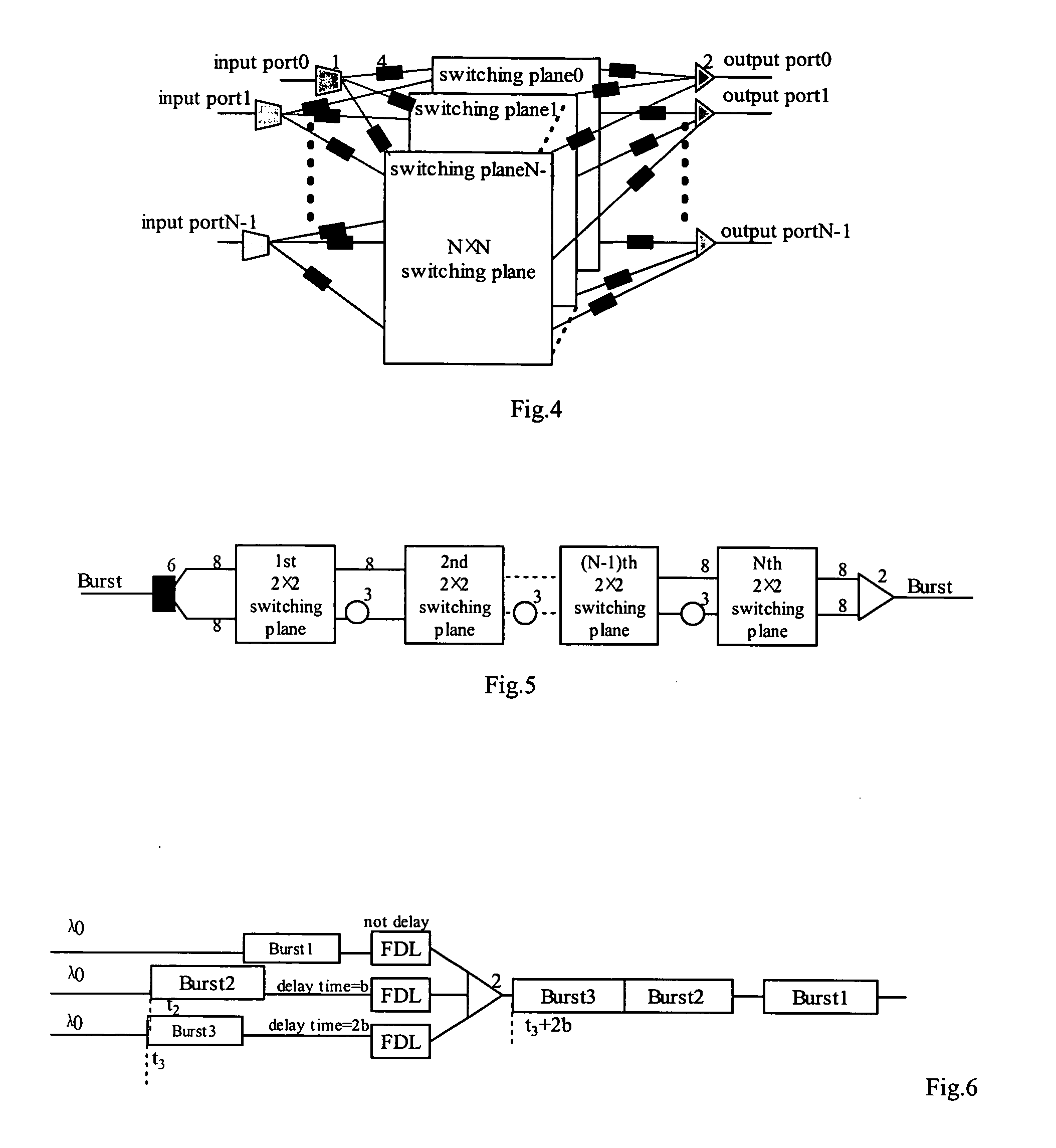
[0037]FIG. 4 is a schematic diagram of the multi-plane OBS node with internal speed-up according to the present invention. The multi-plane OBS node comprises N (N is integer) switching planes 0˜N−1, 2×N2 FDL 4, N 1×N switches 1, N optical couplers 2, N output ports 0˜N−1, and N input ports 0˜N−1. Each input port is connected with a 1×N switch 1 and each output port is the output of its corresponding optical coupler 2. The N switching planes are connected parallelly, wherein a corresponding input of each switching plane is connected with the output of the same corresponding 1×N switch 1 via a respective FDL 4, and a corresponding output of each switching plane is connected with the input of the same corresponding optical coupler 2 via a respective FDL 4.

[0038] It should be noted that among the 2×N2 FDLs 4, N2 FDLs 4 at the input ports are needed only when there are M switching planes (M1 will be replaced by N 1×M switches. It should also be noted that the FDL can be a conventional F...


PUM


Abstract

A multiple-plane OBS node comprises N input ports, N 1×N switches, N switching planes, N2 FDLs, N optical couplers, and N output ports, each input port is connected with the input of a corresponding 1×N switches, the N outputs of each 1×N switch are connected with a corresponding input of each switching plane respectively, a corresponding output of each switching plane is connected with the input of the same corresponding optical coupler via a respective FDL, and each output port is connected with the output of a corresponding optical coupler, wherein N is an integer.

Description

FIELD OF THE INVENTION [0001] The invention relates to optical communication and more specifically to the design of switching architecture and optical buffer of core switching node in Optical Burst Switching. DESCRIPTION OF RELATED ART [0002] Circuit switching and packet switching are two primary technologies for current telecommunication networks. With the rapid development and application of DWDM (Dense Wavelength Divided Multiplex) and relevant optical devices, it is a trend to provide switching capabilities over WDM networks directly. Optical Circuit Switching (also called wavelength routing) has been studied extensively and intensively, and Optical Packet Switching is proposed for the next generation optical Internet. But the two technologies have respective drawbacks. On one side, the exponential growth of the network traffic focuses the interests of future networks on how to support packet traffic or service optimally, which the wavelength routing technology cannot support ef...

Claims


Application Information

Patent Timeline
IPC IPC(8): H04B10/12H04J14/02H04L12/26H04L12/50H04Q3/52H04Q11/00
CPCH04Q11/0005H04Q11/0066H04Q2011/002H04Q2011/0052H04Q2011/0033H04Q2011/0039H04Q2011/005H04Q2011/0024
Inventor WANG, SHENGSONG, HUANXU, DUTAN, WEI
Owner UNIV OF ELECTRONICS SCI & TECH OF CHINA
Why Eureka
Try Eureka