Narrow-body damascene tri-gate FinFET

a tri-gate, narrow-body technology, applied in the field of transistors, can solve the problems of increasing difficulty in overcoming, excessive leakage between the source and drain, and the limitation of conventional methods, and achieve the effects of reducing the resistance of the source/drain series, reducing the design feature below 100 nm, and reducing the design feature of the design feature. below 100 nm,

Active Publication Date: 2005-07-14
ADVANCED MICRO DEVICES INC
View PDF14 Cites 22 Cited by
  • Summary
  • Abstract
  • Description
  • Claims
  • Application Information

AI Technical Summary

Benefits of technology

[0005] Implementations consistent with the present invention provide a narrow-body tri-gate FinFET formed using, for example, a damascene process. A tri-gate FinFET will have better short-channel control than double-gate and single-gate devices, and will have higher drive current than a double-gate finFET for the same area. Local thinning of the fin channel minimizes source / drain series resistance while keeping the short-channel effect under control. The metal tri-gate, formed in a damascene process consistent with the invention, may be used to reduce gate resistance and eliminate poly depletion effects.

Problems solved by technology

The reduction of design features below 100 nm challenges the limitations of conventional methodology.
For example, when the gate length of conventional planar metal oxide semiconductor field effect transistors (MOSFETs) is scaled below 100 nm, problems associated with short channel effects, such as excessive leakage between the source and drain, become increasingly difficult to overcome.
In addition, mobility degradation and a number of process issues also make it difficult to scale conventional MOSFETs to include increasingly smaller device features.

Method used


Image

  • Narrow-body damascene tri-gate FinFET
  • Narrow-body damascene tri-gate FinFET
  • Narrow-body damascene tri-gate FinFET

Examples


Embodiment Construction

[0026] The following detailed description of the invention refers to the accompanying drawings. The same reference numbers in different drawings may identify the same or similar elements. Also, the following detailed description does not limit the invention. Instead, the scope of the invention is defined by the appended claims.

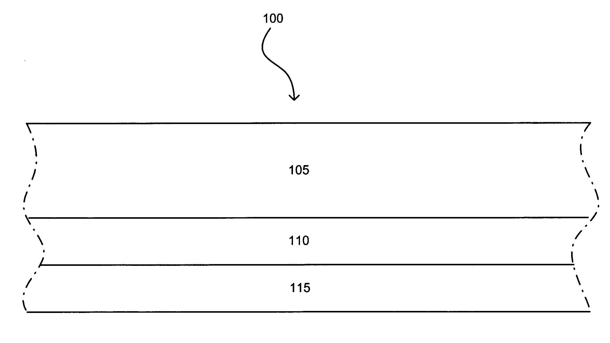
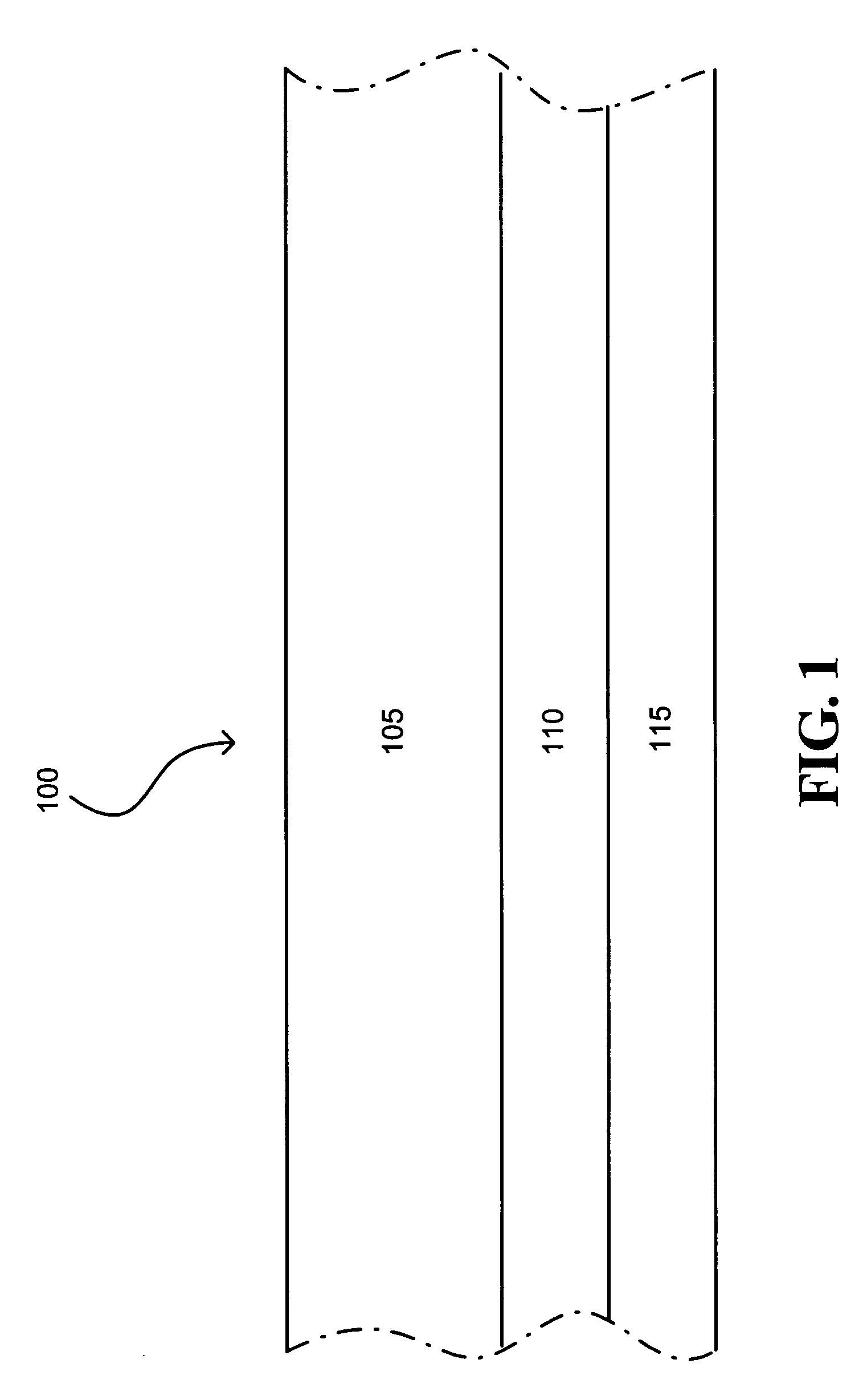
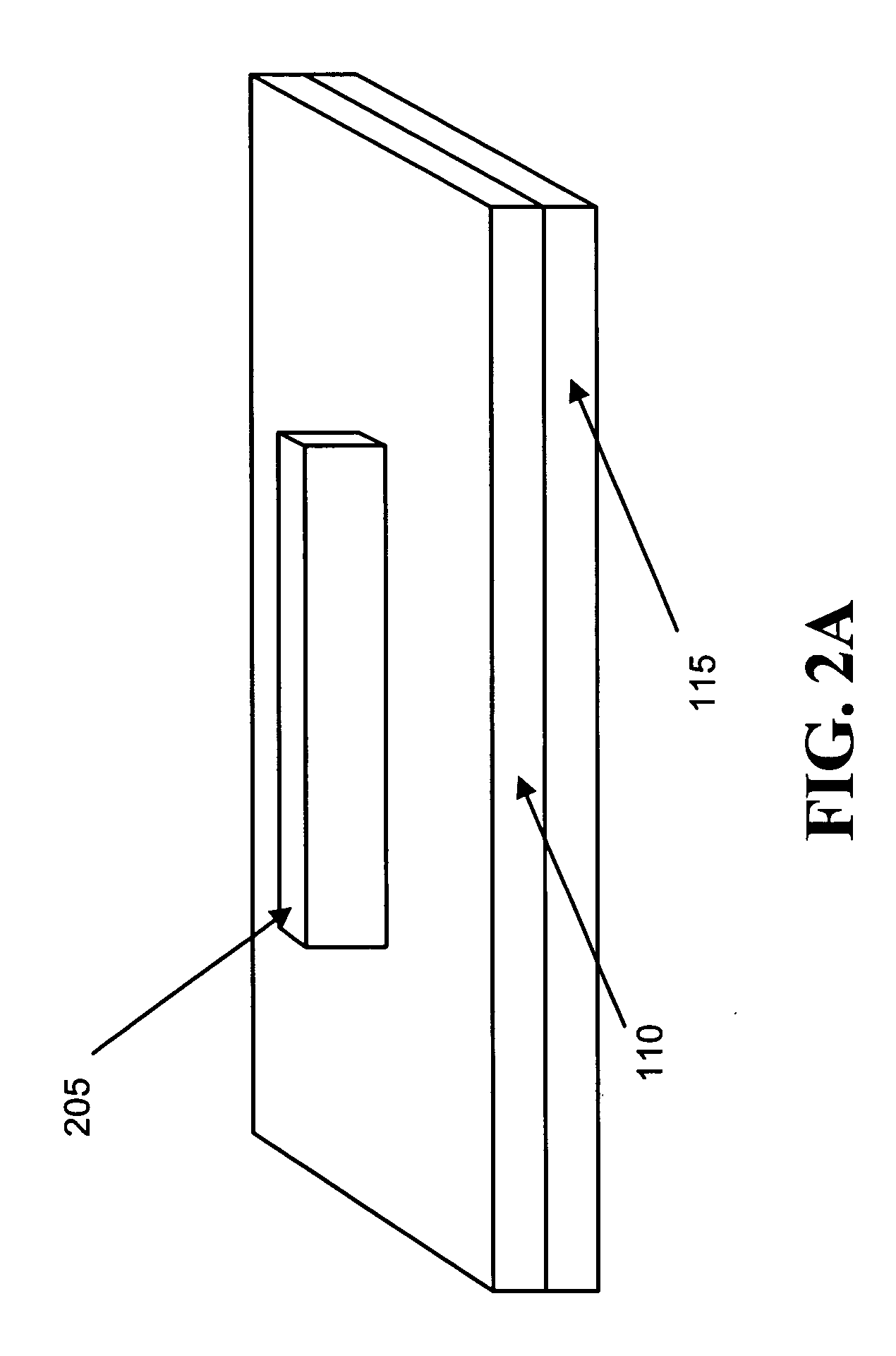
[0027] Consistent with the present invention, an exemplary damascene process for forming a narrow-body tri-gate FinFET is provided. In the exemplary damascene process, a dummy gate may be formed from a layer of crystalline material, such as, for example, polysilicon, that has been formed over a fin. A dielectric layer may then be formed around the dummy gate and over the FinFET fin, source and drain regions. The dummy gate may then be removed to create a gate trench in the dielectric layer. The exposed portions of the FinFET fin within the gate trench may then be locally thinned to reduce source / drain series resistance. A metal gate that contacts three surfac...


PUM


Abstract

A method of forming a fin field effect transistor includes forming a fin and forming a source region on a first end of the fin and a drain region on a second end of the fin. The method further includes forming a dummy gate with a first semi-conducting material in a first pattern over the fin and forming a dielectric layer around the dummy gate. The method also includes removing the first semi-conducting material to leave a trench in the dielectric layer corresponding to the first pattern, thinning a portion of the fin exposed within the trench, and forming a metal gate within the trench.

Description

TECHNICAL FIELD [0001] The present invention relates generally to transistors and, more particularly, to fin field effect transistors (FinFETs). BACKGROUND ART [0002] The escalating demands for high density and performance associated with ultra large scale integration semiconductor devices require design features, such as gate lengths, below 100 nanometers (nm), high reliability and increased manufacturing throughput. The reduction of design features below 100 nm challenges the limitations of conventional methodology. [0003] For example, when the gate length of conventional planar metal oxide semiconductor field effect transistors (MOSFETs) is scaled below 100 nm, problems associated with short channel effects, such as excessive leakage between the source and drain, become increasingly difficult to overcome. In addition, mobility degradation and a number of process issues also make it difficult to scale conventional MOSFETs to include increasingly smaller device features. New device...

Claims


Application Information

Patent Timeline
Patent Type & Authority Applications(United States)
IPC IPC(8): H01L21/336H01L29/786
CPCH01L29/66545H01L29/785H01L29/66795H01L29/78645H01L29/4966
Inventor AHMED, SHIBLY S.WANG, HAIHONGYU, BIN
Owner ADVANCED MICRO DEVICES INC
Why Eureka
Try Eureka