Voltage controlled oscillator

a voltage control and oscillator technology, applied in the direction of pulse generators, pulse techniques, electrical equipment, etc., can solve the problems of increasing cost, large problem, phase noise, etc., and achieve the effect of reducing oscillating frequency fluctuations and low cos

Inactive Publication Date: 2005-07-21
PANASONIC CORP
View PDF2 Cites 18 Cited by
  • Summary
  • Abstract
  • Description
  • Claims
  • Application Information

AI Technical Summary

Benefits of technology

[0024] Therefore, an object of the present invention is to provide a voltage controlled oscillator that has a low cost and has reduced fluctuations in the oscillating frequency.

Problems solved by technology

Therefore, the 1 / f noise converted to a frequency in the vicinity of the oscillating frequency is superimposed on oscillating signals and becomes phase noise.
Therefore, in the conventional voltage control oscillators, occurrence of phase noise in the region A causes a large problem.
Therefore, the chip size of the voltage controlled oscillator is increased, resulting in an increase in the cost.

Method used


Image

  • Voltage controlled oscillator
  • Voltage controlled oscillator
  • Voltage controlled oscillator

Examples


first embodiment

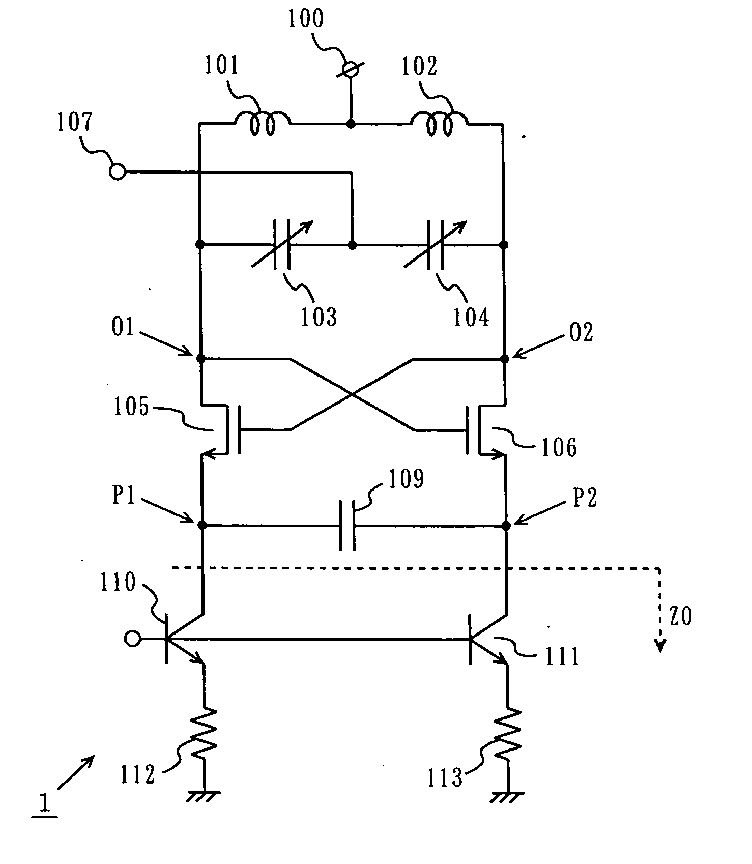
[0081]FIG. 1 is a circuit diagram showing the configuration of a voltage controlled oscillator 1 of a first embodiment of the present invention. In FIG. 1, the voltage controlled oscillator 1 includes a power terminal 100, inductors 101 and 102, variable capacitive elements 103 and 104, oscillating transistors 105 and 106, a frequency control terminal 107, a coupling capacitor 109, current source transistors 110 and 111, and resistors 112 and 113. In FIG. 1, a bias circuit and the like are omitted.

[0082] The variable capacitive elements 103 and 104 utilize the gate capacitance of variable capacitive diodes or field-effect transistors (FET). The oscillating transistors 105 and 106 are field-effect transistors (hereinafter, referred to as “FET”). The coupling capacitor 109 is a capacitor having a predetermined capacitance value. The current source transistor 110 and 111 are bipolar transistors.

[0083] The inductors 101 and 102 are connected in series. The power terminal 100 is connec...

second embodiment

[0104]FIG. 5 is a circuit diagram showing the configuration of a voltage controlled oscillator 2 of a second embodiment of the present invention. In FIG. 5, the voltage controlled oscillator 2 includes a power terminal 100, inductors 101 and 102, variable capacitive elements 103 and 104, oscillating transistors 105 and 106, a frequency control terminal 107, a coupling capacitor 109, current source transistors 110 and 111, resistors 112 and 113, and inductors 120 and 121. In FIG. 5, a bias circuit and the like are omitted. In FIG. 5, the same portions as in the first embodiment bear the same reference numerals and are not described further.

[0105] In the first embodiment, the parasitic capacitance between the emitters and the collectors of the current source transistors 110 and 111 reduces the impedance Z0 as seen from the terminals P1 and P2 to the current source side with respect to higher oscillating frequencies. For example, in the case where the oscillating frequency is 5 GHz, t...

third embodiment

[0118]FIG. 8 is a circuit diagram showing the configuration of a voltage controlled oscillator 3 of a third embodiment of the present invention. In FIG. 8, the voltage controlled oscillator 3 includes a power terminal 100, inductors 101 and 102, variable capacitive elements 103 and 104, oscillating transistors 105 and 106, a frequency control terminal 107, a coupling capacitor 109, current source transistors 110 and 111, and inductors 132 and 133. In FIG. 8, a bias circuit and the like are omitted. In FIG. 8, the same portions as in the first embodiment bear the same reference numerals and are not described further.

[0119] The inductors 132 and 133 are connected between the emitters of the current source transistors 110 and 111 and the ground. The inductors 132 and 133 have an impedance that suppresses a signal with a frequency twice the oscillating frequency at both the terminals of the coupling capacitor 109 similarly to the inductors 120 and 121 in the second embodiment.

[0120] S...


PUM


Abstract

The present invention provides a voltage controlled oscillator for changing an oscillating frequency in accordance an input control voltage, including a parallel resonant circuit, a negative resistance circuit connected in parallel to the parallel resonant circuit, a first capacitor connected in parallel to the negative resistance circuit, a first current source connected between one terminal of the first capacitor and the negative resistance circuit, and a second current source connected between the other terminal of the first capacitor and the negative resistance circuit. The capacitance value of the first capacitor is set to a value that suppresses a signal with a frequency twice the oscillating frequency at both the terminals of the first capacitor. Each of the first and the second current sources is constituted by a bipolar transistor.

Description

BACKGROUND OF THE INVENTION [0001] 1. Field of the Invention [0002] The present invention relates to a voltage controlled oscillator used in wireless communication equipment and PLL circuits. More specifically, the present invention relates to a voltage controlled oscillator in which phase noise can be suppressed. [0003] 2. Description of the Background Art [0004] Voltage controlled oscillators are widely used as means for generating a local oscillating signal of wireless communication equipment. FIG. 19 is a circuit diagram showing the configuration of a conventional voltage controlled oscillator 900. In FIG. 19, the voltage controlled oscillator includes a power terminal 910, inductors 911 and 912, variable capacitive elements 913 and 914, oscillating transistors 915 and 916, a frequency control terminal 917, and a current source transistor 930. In FIG. 19, a bias circuit and the like are omitted. [0005] In FIG. 19, the inductors 911 and 912 and the variable capacitive elements 91...

Claims


Application Information

Patent Timeline
Patent Type & Authority Applications(United States)
IPC IPC(8): H03K3/354
CPCH03K3/354
Inventor TAKINAMI, KOJITSUKIZAWA, TAKAYUKIADACHI, HISASHIOHARA, ATSUSHI
Owner PANASONIC CORP
Why Eureka
Try Eureka