Semiconductor device and method for fabricating the same

a technology of semiconductor devices and semiconductors, applied in semiconductor devices, semiconductor/solid-state device details, electrical apparatus, etc., can solve the problems of pattern scattering, fuses often collapse or are scattered in cleaning, etc., to prevent the spread of fuses, reduce the fuser region, and prevent the effect of fuses from being disconnected

Inactive Publication Date: 2005-07-28
FUJITSU LTD
View PDF11 Cites 46 Cited by
  • Summary
  • Abstract
  • Description
  • Claims
  • Application Information

AI Technical Summary

Benefits of technology

[0017] According to the present invention, the inter-layer insulating film is formed in contact with the sidewall of the fuse in the opening where laser beam is to be irradiated for disconnecting the fuses, whereby the fuse is supported with the inter-layer insulating film. Resultantly, the pattern collapse and the pattern scatter of the fuses in the cleaning following the etching step of forming the opening can be prevented. The direction of the fuses scattering when the fuses are exploded can be restricted in the vertical direction. Resultantly, the wide scatter of the fuses can be prevented, which permits the fuses to be arranged at a small pitch, and the fuser region can be reduced.
[0018] The inter-layer insulating film is formed on the sidewall of the fuse in the opening, whereby the step between the surface of the fuse and the surface of the inter-layer insulating film can be made small. Forming the inter-layer insulating film, covering the entire sidewall of the fuse can make the surface substantially flat in the opening. Resultantly, the generation of residues of the barrier metal in the later bump forming step in the region where laser beam is irradiated for disconnecting the fuses and the generation of residues of the dry film resist in the mounting step can be suppressed. Thus, no residue hinders the disconnection of the fuses.
[0019] The fuse protection film is formed after the opening has been formed, whereby the film thickness of the fuse protection film can be easily controlled to be thin. Resultantly, the fabrication process can be simplified, and the fuses can be stably disconnected.

Problems solved by technology

However, when the cover film or the inter-layer insulating film is etched until the side surfaces of the fuses are completely exposed, the fuses, which are not supported at the side surfaces, the patterns of the fuses often collapse or are scattered in the cleaning step following the etching.
Especially, the inter-layer insulating film directly below the fuses is side-etched, and the fuses overhang, the pattern collapse and the pattern scatter tend to take place.

Method used


Image

  • Semiconductor device and method for fabricating the same
  • Semiconductor device and method for fabricating the same
  • Semiconductor device and method for fabricating the same

Examples


first embodiment

A FIRST EMBODIMENT

[0029] The semiconductor device and the method for fabricating the same according to a first embodiment of the present invention will be explained with reference to FIGS. 1 to 4C.

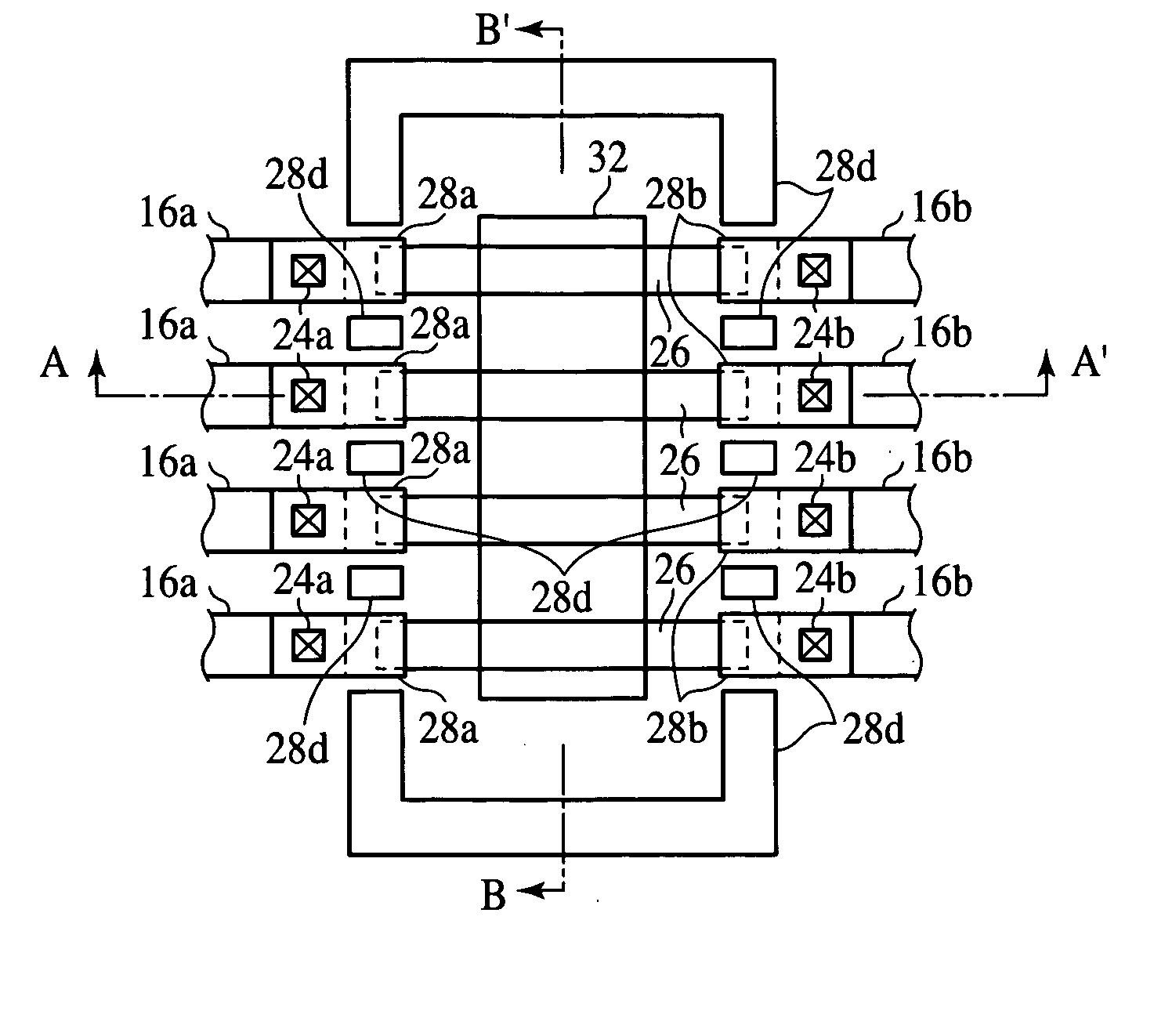
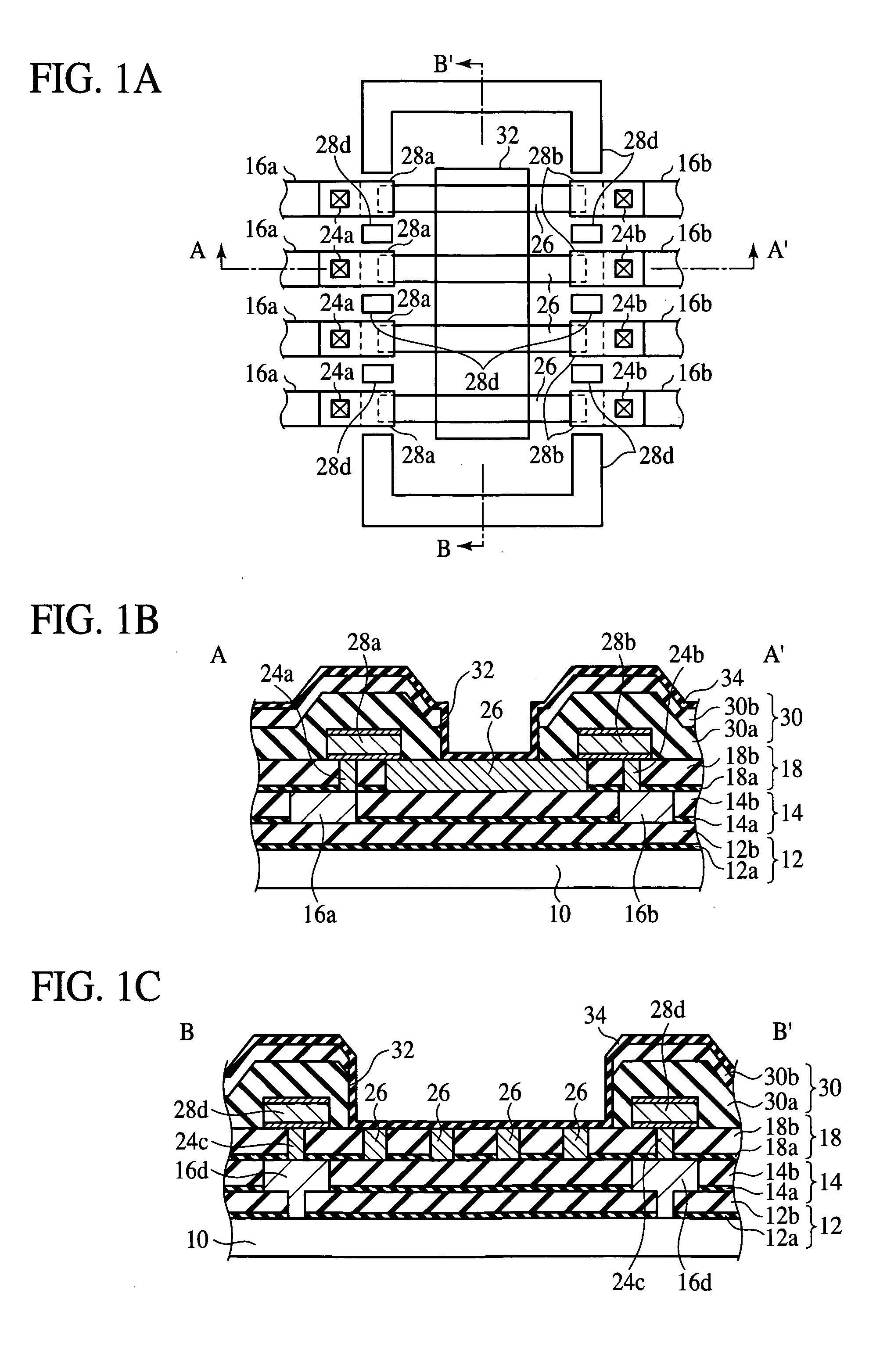
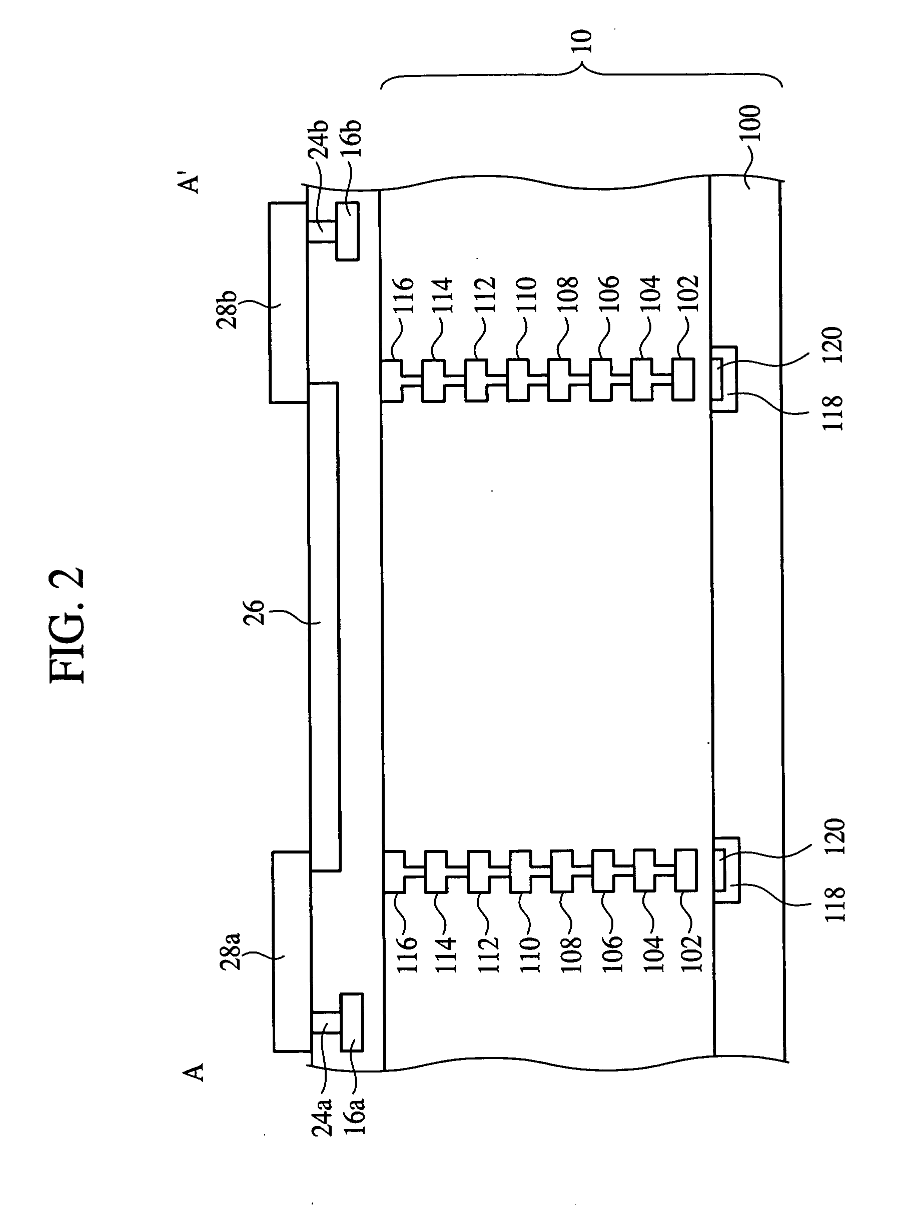
[0030]FIGS. 1A-1C are a plan view and sectional views of the semiconductor device according to the present embodiment, which show the structure thereof. FIG. 2 is a schematic view of the semiconductor device according to the present embodiment, which shows the structure thereof. FIGS. 3A-3E and 4A-4C are sectional views of the semiconductor device according to the present embodiment in the steps of the method for fabricating the same, which show the method.

[0031] First, the structure of the semiconductor device according to the present embodiment will be explained with reference to FIGS. 1A-1C and 2. FIG. 1A is a plan view of the semiconductor device according to the present embodiment, which shows the structure thereof. FIG. 1B is the sectional view along the line A-A′ in FIG. 1. FIG. 1...

second embodiment

A SECOND EMBODIMENT

[0069] The semiconductor device and the method for fabricating the same according to a second embodiment of the present invention will be explained with reference to FIGS. 6A to 8C. The same members of the present embodiment as those of the semiconductor device according to the first embodiment shown in FIGS. 1A to 5 are represented by the same reference numbers not to repeat or to simplify their explanation.

[0070]FIGS. 6A-6C are a plan view and sectional views of the semiconductor device according to the present embodiment, which show the structure thereof. FIGS. 7A-8C are sectional views of the semiconductor device according to the present embodiment in the steps of the method for fabricating the same, which show the method.

[0071] In the first embodiment described above, the present invention is applied to a semiconductor device comprising the fuses formed concurrently with the contact plugs by the so-called damascene process. However, the present invention is...


PUM


Abstract

The semiconductor device comprises an inter-layer insulating film 18 formed over a substrate 10, a fuse 26 buried in the inter-layer insulating film 18, and a cover film 30 formed over the inter-layer insulating film 18 and having an opening formed therein down to the fuse 26. The inter-layer insulating film 18 is formed in contact with the side wall of the fuse 26 in the opening, whereby the fuse 26 is supported with the inter-layer insulating film 18 to thereby prevent the pattern collapse and pattern scatter. The wide scatter of the fuses can be prevented, and the fuses can be arranged in a small pitch.

Description

CROSS-REFERENCE TO RELATED APPLICATIONS [0001] This application is based upon and claims the benefit of priority from the prior Japanese Patent Application No. 2004-015259, filed on Jan. 23, 2004, the entire contents of which are incorporated herein by reference. BACKGROUND OF THE INVENTION [0002] The present invention relates to a semiconductor device and a method for fabricating the same, more specifically a semiconductor device which permits the circuits to be reconstituted by disconnecting fuses by irradiating laser beams and a method for fabricating the semiconductor device. [0003] Semiconductor devices, e.g., memory devices, logic devices, etc., such as DRAM and SRAM, etc., are constituted with a very large number of elements, and often parts of the circuits and memory cells do not normally operate due to various factors caused in the fabrication processes. In such case, if the devices are treated as defects because of the defective partial circuits or memory cells, it will de...

Claims


Application Information

Patent Timeline
Patent Type & Authority Applications(United States)
IPC IPC(8): H01L23/52H01L21/3205H01L21/82H01L23/00H01L23/31H01L23/525H01L27/10
CPCH01L23/3192H01L23/5258H01L23/564H01L27/10H01L2924/0002H01L2924/00H01L21/82
Inventor SATO, MOTONOBUSAWADA, TOYOJIOTSUKA, SATOSHI
Owner FUJITSU LTD
Why Eureka
Try Eureka