Semiconductor device and method of manufacturing the same

a technology of semiconductor devices and semiconductors, applied in semiconductor devices, semiconductor/solid-state device details, electrical apparatus, etc., can solve the problems of low degree of freedom of wiring, large hole size, and large area required, and achieve the effect of increasing the degree of wiring freedom and enhancing functionality

Active Publication Date: 2005-07-28
SHINKO ELECTRIC IND CO LTD
View PDF14 Cites 128 Cited by
  • Summary
  • Abstract
  • Description
  • Claims
  • Application Information

AI Technical Summary

Benefits of technology

[0010] An object of the present invention is to provide a semiconductor device and a method of manufacturing the semiconductor device in which when a semiconductor element (chip) is mounted within a package, miniaturization is realized and the degree of freedom of wiring is increased, in which a three-dimensional arrangement configuration of chips and connections therebetween can be easily realized as needed, and consequently which contributes to an enhancement of functionality.
[0012] In the semiconductor device according to this aspect, the semiconductor element (chip) is buried and mounted within the wiring board used as a package, and the via hole piercing the wiring board vertically (in the thickness direction) is formed in a region around the chip. The via hole can be formed to have a small diameter, for example, by laser processing, compared with a through hole formed by drilling as heretofore. This means that an area required around the chip can be relatively reduced, and contributes to a miniaturization of the package (semiconductor device).
[0013] Moreover, since the via hole is filled with the conductor, the first pad portion (top-and-bottom connecting pad) can be placed thereon (on one end of the conductor). Namely, compared with the case where a plated through hole is formed as heretofore and where a top-and-bottom connecting pad cannot be placed thereon and must be formed at another position, the degree of freedom of wiring can be increased. Further, since the relevant pad does not need to be formed at another position, an area required around the chip can be accordingly reduced. This contributes to a further miniaturization of the package (semiconductor device).
[0014] Furthermore, devices according to the present aspect can be stacked in a multilayered manner by using the first and second pad portions respectively exposed from both surfaces of the package (semiconductor device) as top-and-bottom connecting pads, and as needed, by interposing external connection terminals therebetween. Accordingly, it is possible to easily realize a three-dimensional arrangement configuration of chips and connections therebetween. This contributes to an enhancement of functionality.

Problems solved by technology

Consequently, the diameters of the through holes become relatively large (approximately 250 to 300 μm in the state of the art), and there has been a disadvantage in that a larger area is accordingly required.
Further, there are constraints on design (i.e., the degree of freedom of wiring is low), such as the technical difficulty of placing top-and-bottom connecting pads on plated through holes.
This has become an obstacle to miniaturization.
However, the above-described problem becomes a serious obstacle to the accomplishment of this purpose.

Method used


Image

  • Semiconductor device and method of manufacturing the same
  • Semiconductor device and method of manufacturing the same
  • Semiconductor device and method of manufacturing the same

Examples


first embodiment

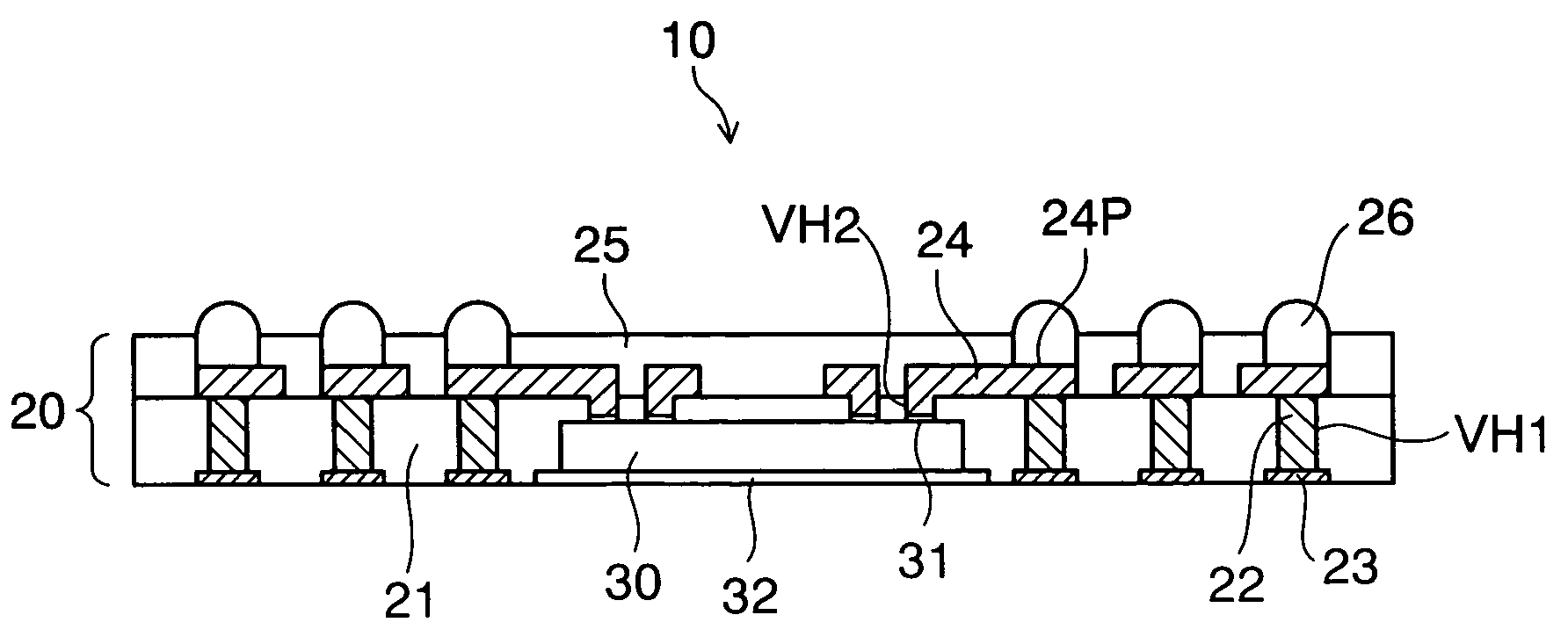
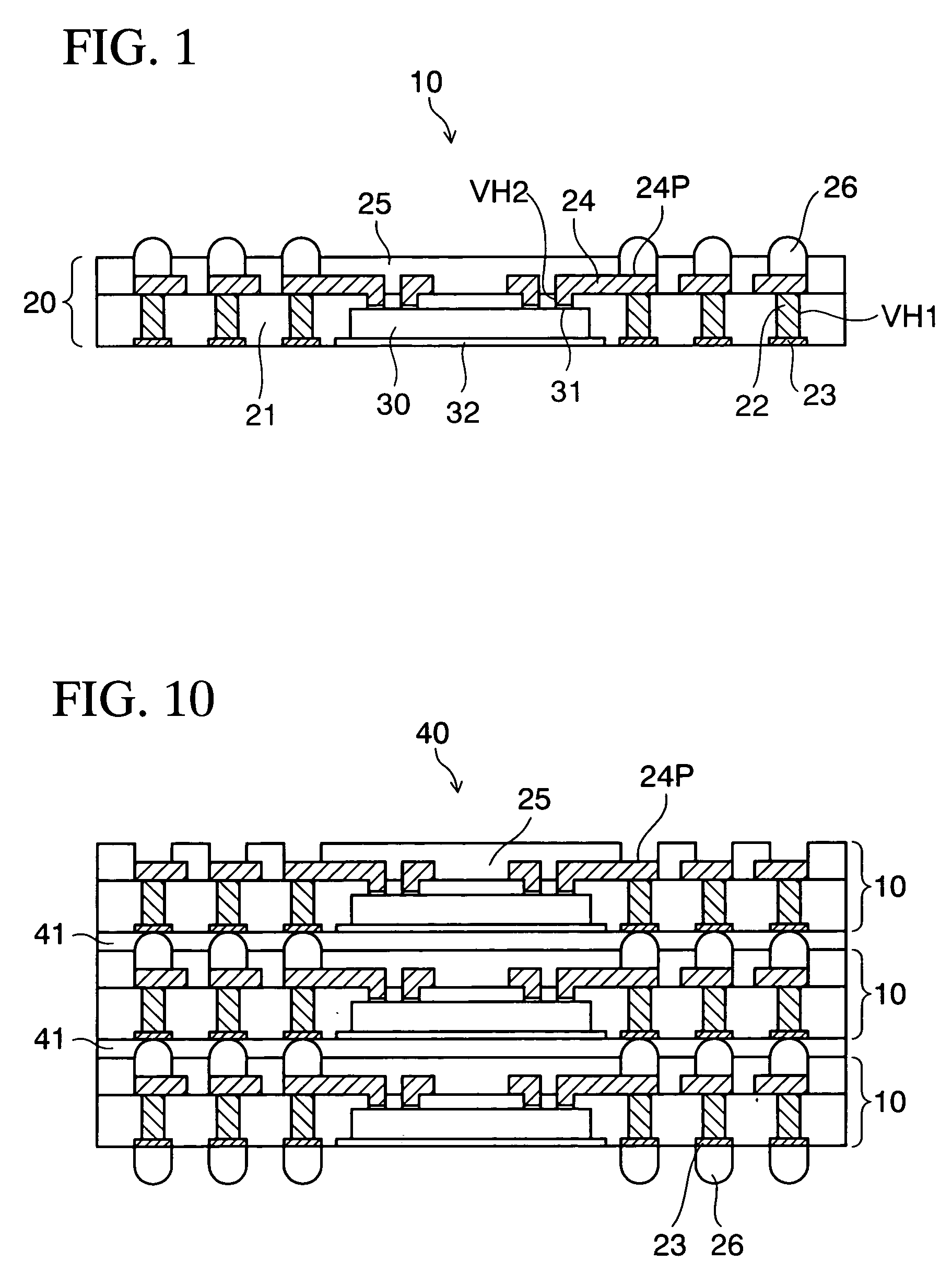
[0029]FIG. 1 schematically shows a cross-sectional structure of a semiconductor device according to the present invention.

[0030] The semiconductor device 10 according to this embodiment includes a wiring board 20 used as a package, and a semiconductor element (silicon (Si) chip) 30 buried in the package (wiring board) 20. In the example shown in the drawing, one semiconductor chip 30 is buried in one package. However, two or more semiconductor chips 30 may be appropriately buried therein depending on functions required for the present device 10.

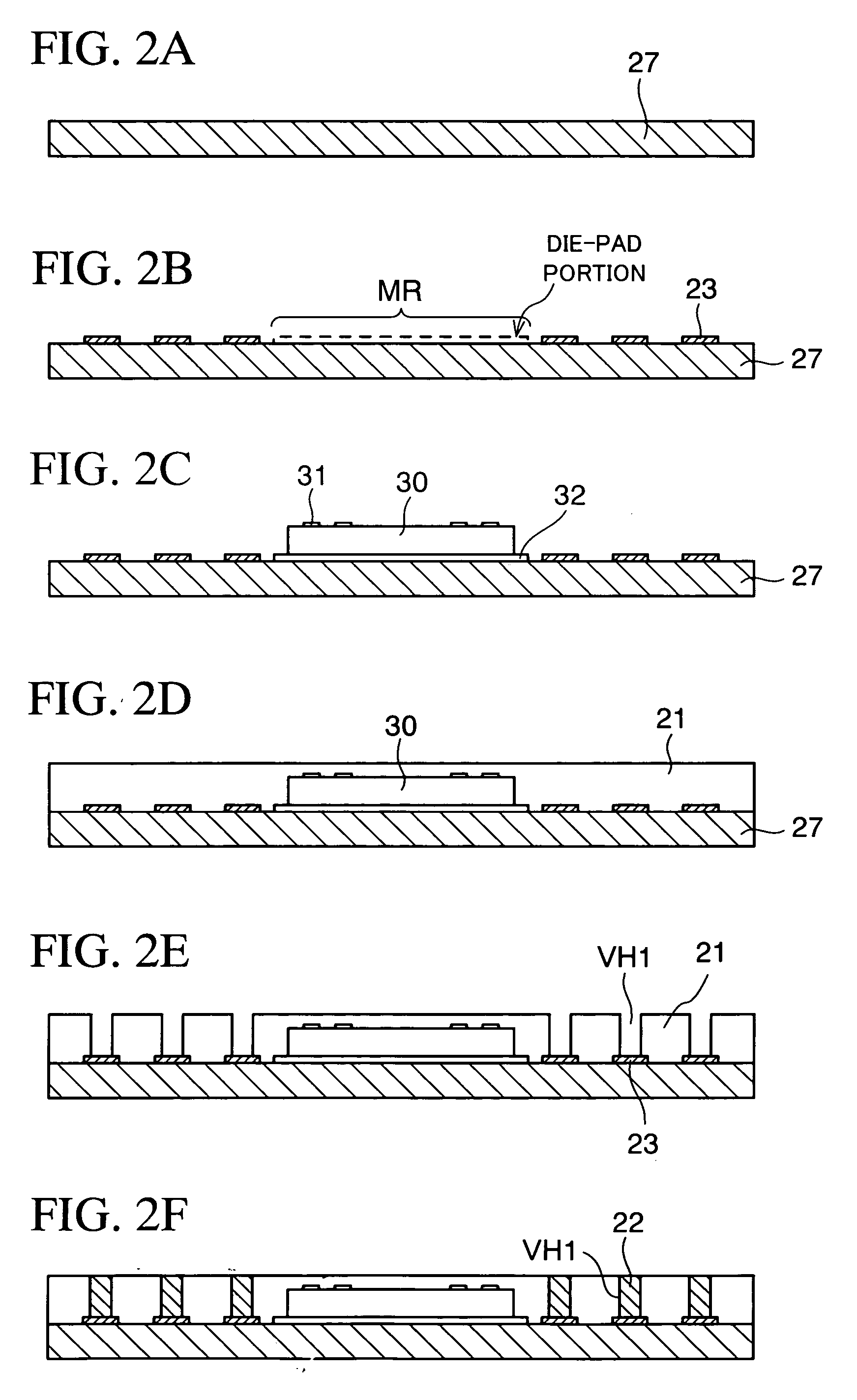
[0031] In the package (wiring board) 20, reference numeral 21 denotes an insulating base material (e.g., a resin layer made of epoxy resin) which serves as a base for the wiring board. In this resin layer 21, via holes VH1 piercing the resin layer 21 in the thickness direction are formed in a region around the semiconductor chip 30. These via holes VH1 are filled with conductors 22 (e.g., metal such as copper (Cu)). At one end (lower surface...

second embodiment

[0053]FIG. 4 schematically shows a cross-sectional structure of a semiconductor device according to the present invention.

[0054] In this embodiment, similar to the first embodiment (FIG. 1), the semiconductor device 10a includes a wiring board 20a used as a package, and the semiconductor chip 30 buried in the package (wiring board) 20a. The package (wiring board) 20a in this embodiment differs from the package (wiring board) 20 in the first embodiment in that a resin layer 21a is formed in such a manner that the exposed surface of the insulating layer 32 protrudes from one surface (surface in which the pad portions 23 are formed) of the resin layer 21a. Other components and functions thereof are the same as those of the first embodiment, and thus the explanation thereof is omitted.

[0055] Further, in a method of manufacturing the semiconductor device 10a of this embodiment, part of manufacturing steps thereof are also different because of the features of the above-described constitu...

third embodiment

[0057]FIG. 7 schematically shows a cross-sectional structure of a semiconductor device according to the present invention.

[0058] In this embodiment, similar to the second embodiment (FIG. 4), the semiconductor device 10b includes a wiring board 20b used as a package, and the semiconductor chip 30 buried in the package (wiring board) 20b. The package (wiring board) 20b in this embodiment differs from the package (wiring board) 20a in the second embodiment in that one end of the conductor 22b filled in the via hole VH1 protrudes from one surface (lower surface in the example shown in the drawing) of a resin layer 21b, and that the pad portion 23b is formed to follow the shape of the protruded surface (convex surface) of the conductor 22b. Other components and functions thereof are the same as those of the second embodiment, and thus the explanation thereof is omitted.

[0059] Further, in a method of manufacturing the semiconductor device 10b of this embodiment, part of manufacturing st...


PUM


Abstract

In a semiconductor device, via holes are formed around a chip buried in a package, one end of a conductor filled in the via hole is covered with a pad portion exposed to the outside, and a wiring layer connected to the other end of the conductor is formed. The portion (pad portion) of the wiring layer which correspond to the conductor is exposed from a protective film, or an external connection terminal is bonded to the top of the pad portion. Electrode terminals of the chip are connected to the wiring layer, and the opposite surface of the chip is exposed to the outside.

Description

CROSS-REFERENCE TO RELATED APPLICATIONS [0001] This application is based on and claims priority of Japanese Patent Application No. 2004-011666 filed on Jan. 20, 2004, the entire contents of which are incorporated herein by reference. BACKGROUND OF THE INVENTION [0002] (a) Field of the Invention [0003] The present invention relates to a semiconductor device and a method of manufacturing the same. More specifically, the present invention relates to a semiconductor device having a package structure in which a semiconductor element (chip) is mounted within a wiring board for a reduction in thickness, and relates to a method of manufacturing the same. [0004] (b) Description of the Related Art [0005] Heretofore, semiconductor devices having various forms have been proposed in which a chip is mounted within a wiring board. As an example, there is a package structure (semiconductor device) intended to form a required circuit block by incorporating and stacking a plurality of chips, for exam...

Claims


Application Information

Patent Timeline
Patent Type & Authority Applications(United States)
IPC IPC(8): H01L21/4763H01L21/60H01L25/18H01L21/68H01L23/48H01L23/498H01L23/538H01L25/10H01L25/11
CPCH01L21/568H01L21/6835H01L2924/10253H01L23/49816H01L23/49827H01L23/5389H01L24/19H01L25/105H01L2221/68345H01L2221/68359H01L2224/04105H01L2224/20H01L2224/211H01L2224/92244H01L2924/01029H01L2924/01046H01L2924/01078H01L2924/01079H01L2924/15311H01L2924/15331H01L2924/01005H01L2924/01006H01L2924/01033H01L2924/1815H01L2225/1035H01L2225/1058H01L2924/00H01L2924/12042H01L2224/12105
Inventor TAKEUCHI, YUKIHARUTAKAYANAGI, HIDENORI
Owner SHINKO ELECTRIC IND CO LTD
Why Eureka
Try Eureka