Vapor phase growth method for al-containing III-V group compound semiconductor, and method and device for producing al-containing IIl-V group compound semiconductor

a compound semiconductor and growth method technology, applied in the direction of crystal growth process, polycrystalline material growth, chemically reactive gas, etc., can solve the problems of difficult substrate fabrication, inability to achieve other semiconductors, and large amount of time to form a thick layer of 100 microns or thicker

Inactive Publication Date: 2005-08-04
NOKODAI TLO KK
View PDF6 Cites 38 Cited by
  • Summary
  • Abstract
  • Description
  • Claims
  • Application Information

AI Technical Summary

Benefits of technology

The objective of this patent is to create a way to make materials called Al-containing III-V group compounds using a process called HVPE (hydrogen vapor phase epitaxy). This method allows for large scale production of these materials. By doing this, researchers hope to prevent cracks from forming when they grow layers of material like aluminum gallium nitride on top of other materials with different properties. These cracks are often caused because there is a big difference in how much each material expands or contracts with changes in temperature. If we can avoid these cracks, then more applications could be possible using these new materials.

Problems solved by technology

The technical problem addressed in this patent text relates to finding ways to produce high quality LED lights and other electronic components containing Al-containingIII-V group compound semiconductors without causing cracking or contamination during the manufacturing process. Current methods like LPE, MBE, and MOVPE all face limitations in terms of forming thick layers and achieving consistent purity levels. Additionally, traditional methods like HVPE suffer from issues related to the difficulty of producing uniform layers across larger areas and damage to the underlying substrate.

Method used


Image

  • Vapor phase growth method for al-containing III-V group compound semiconductor, and method and device for producing al-containing IIl-V group compound semiconductor
  • Vapor phase growth method for al-containing III-V group compound semiconductor, and method and device for producing al-containing IIl-V group compound semiconductor
  • Vapor phase growth method for al-containing III-V group compound semiconductor, and method and device for producing al-containing IIl-V group compound semiconductor

Examples


example 1

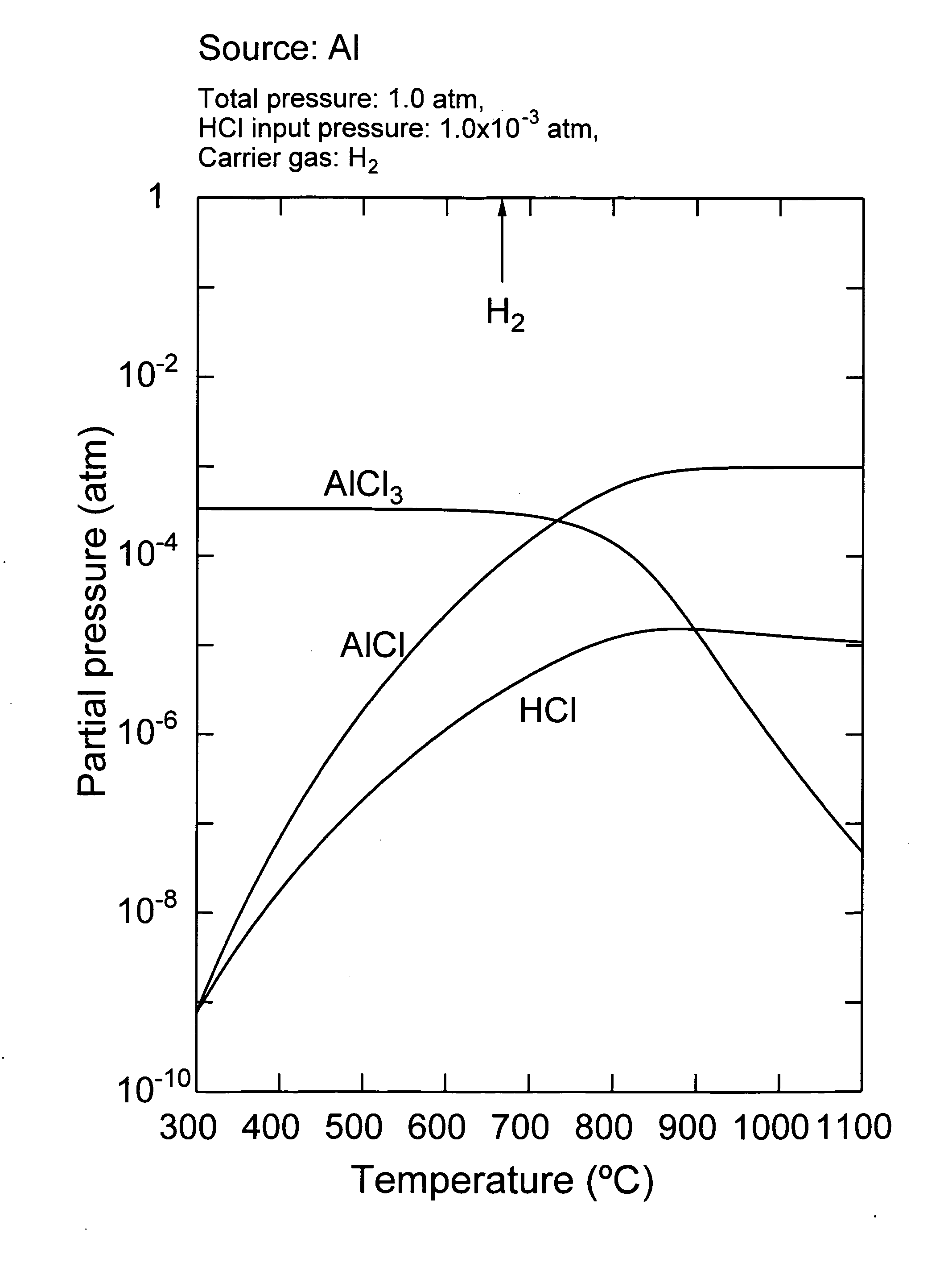
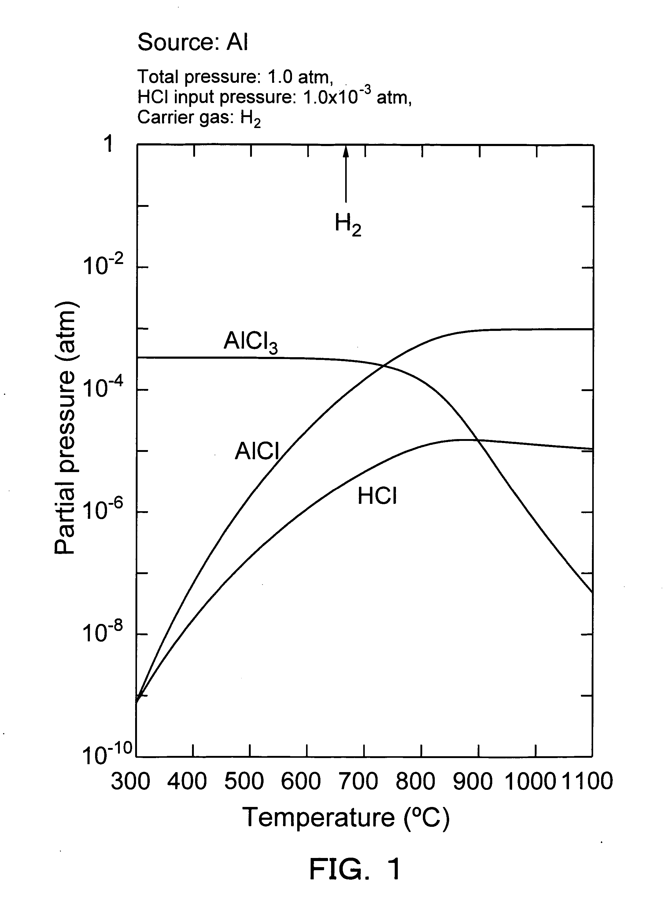
[0062]FIG. 5 shows one exemplary construction according to the present invention, in which the temperature of the Al material area was set to 650° C., and HCl and hydrogen were introduced into the Al material area with the temperature of the crystallization area set to 1000° C. FIG. 5 is a photograph showing the crystallization area of the reaction tube 5 hours after the experiment was started. Consistent with the previous discussion, substantially no aluminum monochloride (AlCl), the reactive species, was generated in the Al material area kept at 650° C. and the Al component was transported in the form of AlCl3. As can be seen from the photograph, the quartz reaction tube exhibited no color change, demonstrating that the Al component can be transported without reacting with the quartz reaction tube by maintaining the temperature of the Al material area in the range of 300° C. to 700° C., the range specified by the present invention.

example 2

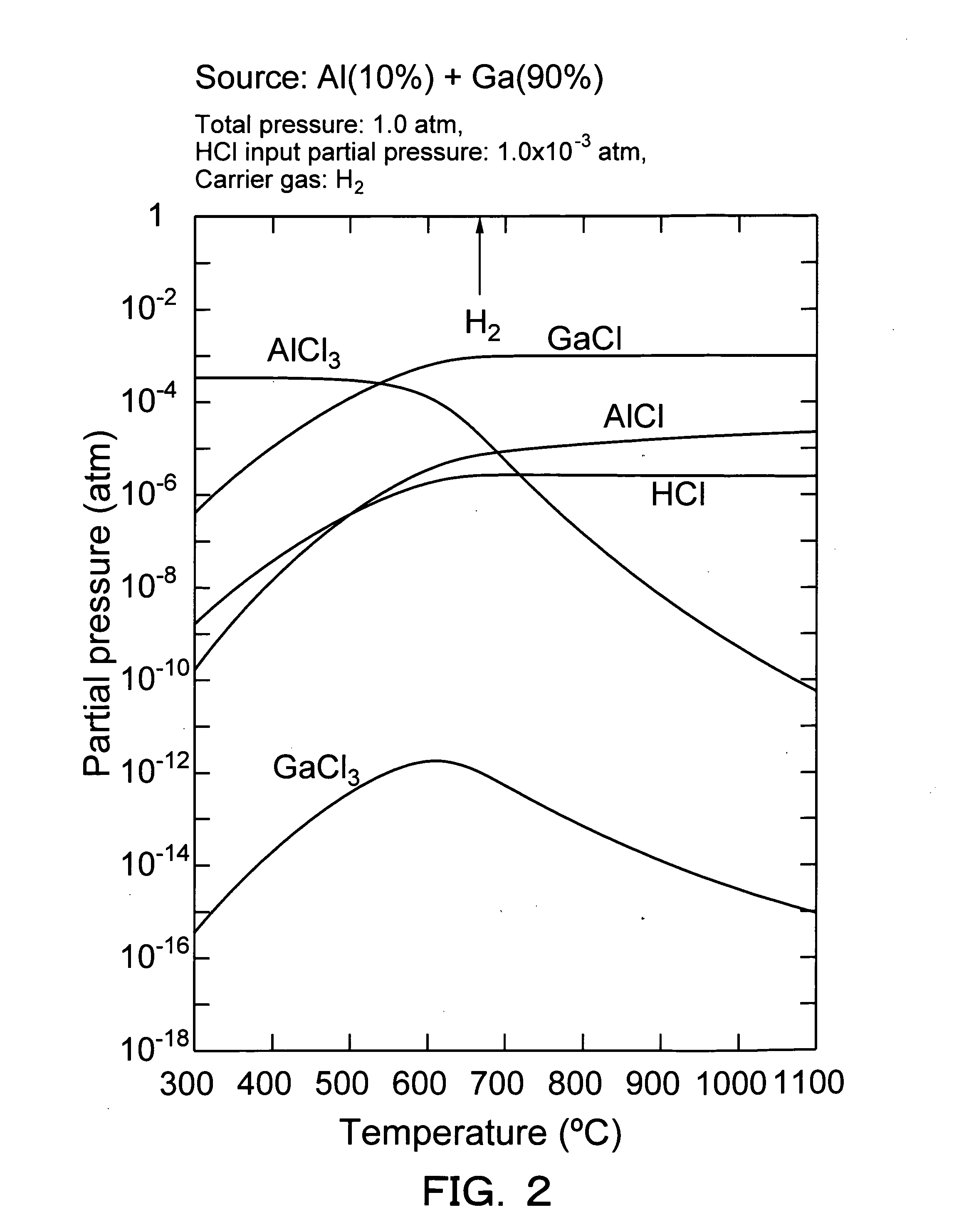
[0063] Using the vapor phase growth apparatus shown in FIG. 3, epitaxial growth of AlN was carried out. Specific growth process was as follows: First, HCl was introduced along with hydrogen to serve as the carrier gas while the Al material area was maintained at 650° C. NH3 and hydrogen to serve as the carrier gas were introduced while the temperature of the adjacent area of the Si substrate was varied from 900 to 1100° C. As a result, the reaction of AlCl3 with NH3 took place in the crystallization area in the vicinity of the Si substrate to cause the AlN crystal to epitaxially grow on the Si substrate.

[0064] The growth experiment was conducted in replicates with different HCl input partial pressures ranging from 1×10⁻⁴ atm to 5×10⁻² atm and different NH3 input partial pressures of 0.1, 0.2, 0.4, and 0.5 atm. As a result, it was proven that an AlN layer with high crystal quality was epitaxially grown on the Si substrate when the temperature of the Al material area was about 600° C...


PUM

PropertyMeasurementUnit
Temperatureaaaaaaaaaa
Speedaaaaaaaaaa

Abstract

A method for growing a crystal of an Al-containing III-V group compound semiconductor by the conventional HVPE method, characterized in that it comprises a step of reacting Al with hydrogen halide at a temperature of 700° C. or lower to form a halide of Al. The method has allowed the suppression of the formation of aluminum chloride (AlCl) or aluminum bromide (AlBr) reacting violently with quartz, which is the material of a reaction vessel for the growth, resulting in the achievement of the vapor phase growth of an Al-containing III-V group compound semiconductor at a rate of 100 microns/hr or more, which has lead to the mass-production of a substrate and a semiconductor element having satisfactory resistance to adverse environment.

Description


Claims


Application Information

Patent Timeline
Owner NOKODAI TLO KK
Why Eureka
Try Eureka