Semiconductor device and manufacturing method thereof

a technology of semiconductor devices and manufacturing methods, applied in semiconductor devices, electrical devices, transistors, etc., can solve the problems of large parasitic capacity generated in the gate electrode by the depletion of the gate electrode, and the thickness of the gate insulating film has become smaller

Active Publication Date: 2005-08-04
RENESAS ELECTRONICS CORP +2
View PDF8 Cites 29 Cited by
  • Summary
  • Abstract
  • Description
  • Claims
  • Application Information

AI Technical Summary

Problems solved by technology

However, in recent years, the thickness of a gate insulating film has become smaller along with the scaling down of a CMOS transistor, and the depletion of a gate electrode when a polysilicon film is used for a gate electrode has become non-negligible.
However, in this case, a parasitic capacity generated in the gate electrode by the depletion of the gate electrode becomes so large that cannot be neglected.
In addition, in the p-type MIS transistor, the metal constituting the gate electrode is peeled from the gate insulating film and metal atoms are diffused in the gate insulating film and the silicon substrate by the high-temperature heat treatment, and the electrical properties of the MIS transistor are degraded disadvantageously.

Method used


Image

  • Semiconductor device and manufacturing method thereof
  • Semiconductor device and manufacturing method thereof
  • Semiconductor device and manufacturing method thereof

Examples


first embodiment

(First Embodiment)

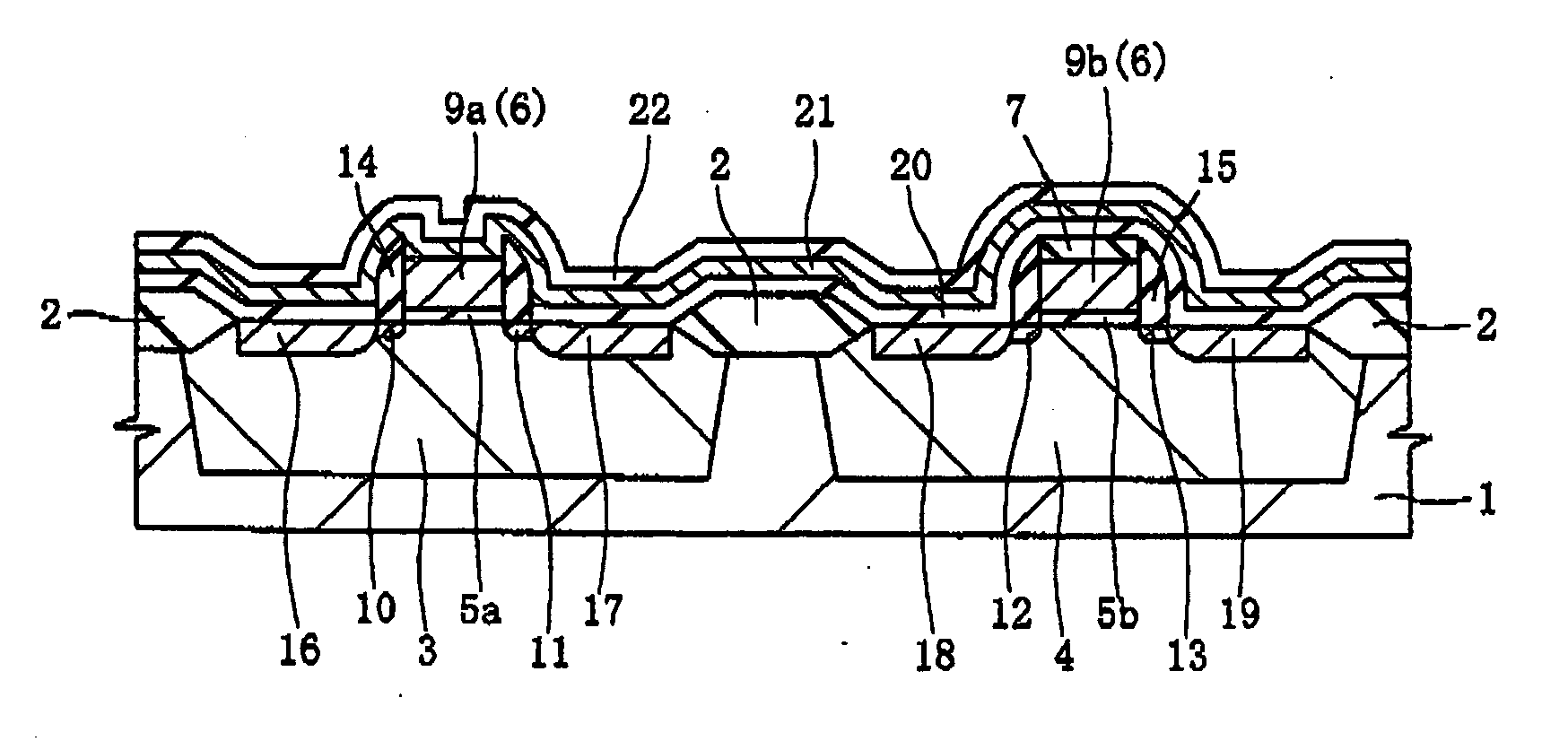
[0043]FIG. 1 is a cross-sectional view showing an n-channel MIS transistor Q1 (referred to as an n-type MIS transistor Q1 hereinafter) and a p-channel MIS transistor Q2 (referred to as a p-type MIS transistor Q2 hereinafter) according to a first embodiment. In FIG. 1, element isolation regions 2 for isolating elements are formed on a semiconductor substrate 1, and a p-type well 3 and an n-type well 4 are formed in active regions isolated by the element isolation regions 2.

[0044] The n-type MIS transistor Q1 is formed on the p-type well 3, and the p-type MIS transistor Q2 is formed on the n-type well 4.

[0045] The n-type MIS transistor Q1 has a gate insulating film (first gate insulating film) 5a composed of, for example, a silicon oxide film and a gate electrode (first gate electrode) 24a on the gate insulating film 5a. The gate electrode 24a is formed of, for example, a hafnium silicide film 23. Since the value of work function of the hafnium silicide film 23 is ...

second embodiment

(Second Embodiment)

[0088] In the first embodiment, the case where a metal silicide film is used as a gate electrode has been described. Meanwhile, in the description of the second embodiment, a film of the same type as that of a metal silicide film constituting a gate electrode is formed on a source region and a drain region.

[0089]FIG. 14 is a cross-sectional view showing an n-type MIS transistor Q3 and a p-type MIS transistor Q4 according to the second embodiment. In FIG. 14, since the configuration of the n-type MIS transistor Q3 and the p-type MIS transistor Q4 is almost the same as that of the n-type MIS transistor Q1 and the p-type MIS transistor Q2 according to the first embodiment, only the different parts will be described below.

[0090] The n-type MIS transistor Q3 according to the second embodiment is different from the n-type MIS transistor Q1 according to the first embodiment in that hafnium silicide films 36 and 37 are formed on high-concentration n-type impurity diffus...

third embodiment

(Third Embodiment)

[0106] In the description of the second embodiment, the same metal silicide films as metal silicide films constituting gate electrodes are formed on the source region and the drain region in the n-type MIS transistor and the p-type MIS transistor. Meanwhile, in the third embodiment, the case where metal silicide films formed on a source region and a drain region of an n-type MIS transistor are formed of the same films as metal silicide films formed on a source region and a drain region of a p-type MIS transistor will be described.

[0107]FIG. 21 is a cross-sectional view showing an n-type MIS transistor Q5 and a p-type MIS transistor Q6 according to the third embodiment. In FIG. 21, since the configuration of the n-type MIS transistor Q5 is almost the same as that of the n-type MIS transistor Q3 according to the second embodiment, only the different parts will be described below.

[0108] The n-type MIS transistor Q5 according to the third embodiment is different from...


PUM


Abstract

A technique capable of reducing threshold voltage and reducing high-temperature heat treatment after forming a gate electrode is provided. An n-type MIS transistor or a p-type MIS transistor is formed on an active region isolated by an element isolation region of a semiconductor substrate. In the n-type MIS transistor, a gate electrode is formed through a gate insulating film, and the gate electrode is composed of a hafnium silicide film. On the other hand, in the p-type MIS transistor, a gate electrode is formed through a gate insulating film, and the gate electrode is composed of a platinum silicide film. Also, the gate electrodes are formed after the activation annealing (heat treatment) for activating impurities implanted into a source region and a drain region.

Description

CROSS-REFERENCE TO RELATED APPLICATION [0001] The present application claims priority from Japanese Patent Application JP 2004-023568 filed on Jan. 30, 2004, the content of which is hereby incorporated by reference into this application. TECHNICAL FIELD OF THE INVENTION [0002] The present invention relates to a semiconductor device and a manufacturing technique thereof. More particularly, it relates to the technique for reducing a threshold voltage which is effective when applied to a MIS (Metal Insulator Semiconductor) transistor and a manufacturing technique thereof. BACKGROUND OF THE INVENTION [0003] In a conventional technique, in order to achieve the low threshold voltage in both an n-type MOS transistor and a p-type MOS transistor of a CMOS (Complementary Metal Oxide Semiconductor) transistor, a so-called dual gate structure in which the gate electrodes are formed of materials having different work functions (Fermi potential in the case of polysilicon) has been employed. More ...

Claims


Application Information

Patent Timeline
IPC IPC(8): H01L21/28H01L21/336H01L21/768H01L21/8238H01L27/092H01L29/423H01L29/49H01L29/51H01L29/76H01L29/78H01L29/94H01L31/062H01L31/113H01L31/119
CPCH01L21/28176H01L21/28202H01L21/823835H01L21/823842H01L29/6659H01L29/517H01L29/518H01L29/665H01L29/66545H01L29/51
Inventor KADOSHIMA, MASARUAKIYAMA, KOJIOHNO, MORIFUMI
Owner RENESAS ELECTRONICS CORP
Why Eureka
Try Eureka