Tip structure of platinum-platinum silicide-silicon composite field sensor probe and method for forming MSTA strucutre on the probe

a composite field sensor and platinum-platinum silicide technology, applied in scanning probe microscopy, instruments, measurement devices, etc., can solve the problems of imposing a challenge to mass production, stray field effect (sfe) not being avoided, limited nano-level properties measured, etc., to enhance the spatial resolution and sensitivity of the tip, and enhance the spatial resolution of the field sensor.

Active Publication Date: 2016-02-09
NAT APPLIED RES LAB
View PDF4 Cites 0 Cited by
  • Summary
  • Abstract
  • Description
  • Claims
  • Application Information

AI Technical Summary

Benefits of technology

[0005]It is a main and the other objects of the present invention to provide a tip structure of a platinum-platinum silicide-silicon composite field sensor probe, and a method for forming a modified silicon tip apex (MSTA) structure on the probe, respectively, where a chemical deposition method is used in combination with a microwave annealing process so that a local platinum silicide layer is formed between a platinum nano-structure and a silicon probe tip with a good spatial resolution and sensitivity, which may largely enhance a tip conductivity and a field sensor spatial resolution.
[0006]According to the present invention, the tip structure of a platinum-platinum silicide-silicon composite field sensor probe comprises a silicon probe tip; a platinum nano-structure, growing on the silicon probe tip; and a local platinum silicide layer, disposed between the silicon probe tip and the platinum nano-structure to increase a tip field sensor resolution ability.

Problems solved by technology

Although they may present the properties of the material such as a local surface potential, an electric field, and a magnetic field, the properties measured for the nano-level are limited by the spatial resolution.
Since the tip has an exceedingly large field detection cross-section, the stray-field effect (SFE) may not be avoided.
However, the above cited technologies with the energy beam or dry etch basis require a rigorous vacuum equipment, imposing a challenge to a mass production.
However, the issue of a low transmission efficiency of the electrons between the metal and the silicon probe is all encountered in the electro-coating, the electro-coating free and the electron beam induced deposition (EBID), adversely affecting a field detection efficiency.
However, the prior art forms the metal silicide mostly by using an annealing process in the conventional furnace tube, and hence an overall heating policy has a large effect on the overall nano-level device and only few local tip annealing report may be seen.
Although the inventor of this patent application has proposed a technology for forming the modified silicon tip apex by Ag along with a microwave annealing process to enhance the field detection ability in 2013, Ag is apt to be vulcanized or oxidized in an ambient environment, badly affecting a lifetime of the probe and further imposing an unfavorable effect on actual applications in the semiconductor industry.
Therefore, the prior art may not meet the requirement of the actual use.

Method used


Image

  • Tip structure of platinum-platinum silicide-silicon composite field sensor probe and method for forming MSTA strucutre on the probe
  • Tip structure of platinum-platinum silicide-silicon composite field sensor probe and method for forming MSTA strucutre on the probe
  • Tip structure of platinum-platinum silicide-silicon composite field sensor probe and method for forming MSTA strucutre on the probe

Examples


Embodiment Construction

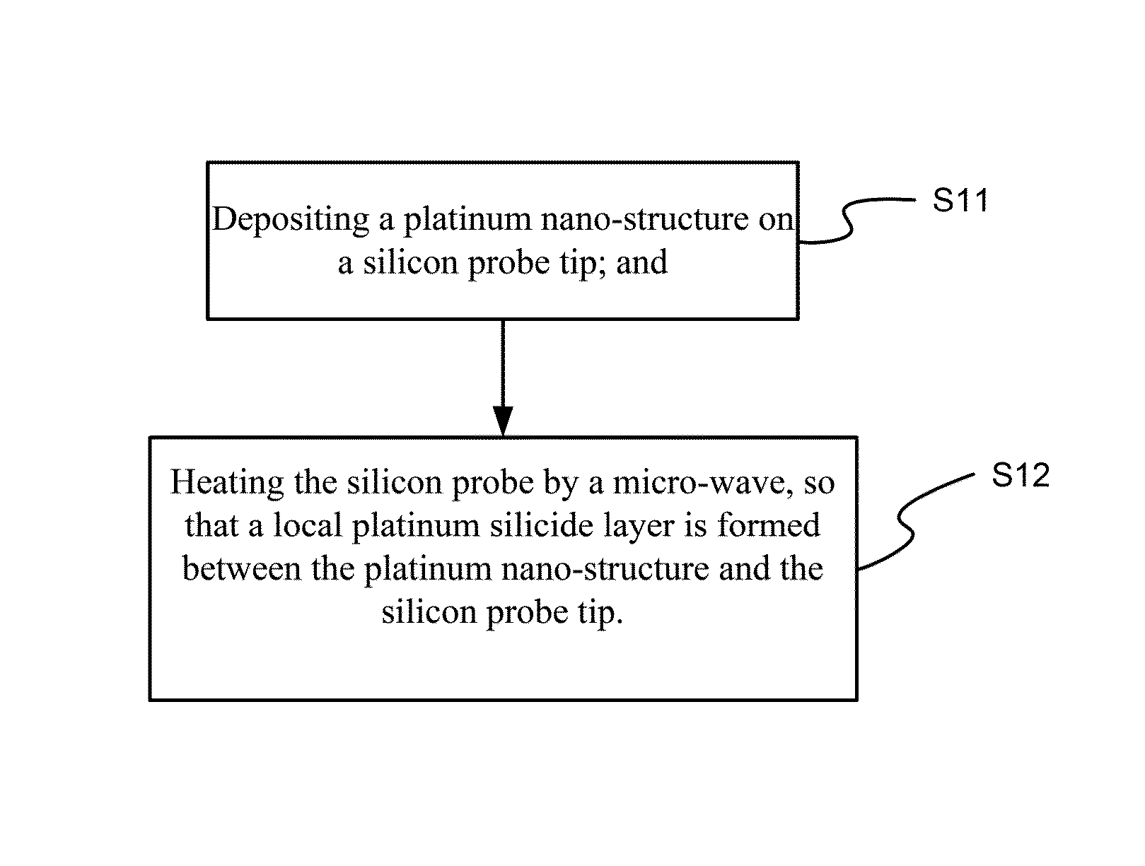
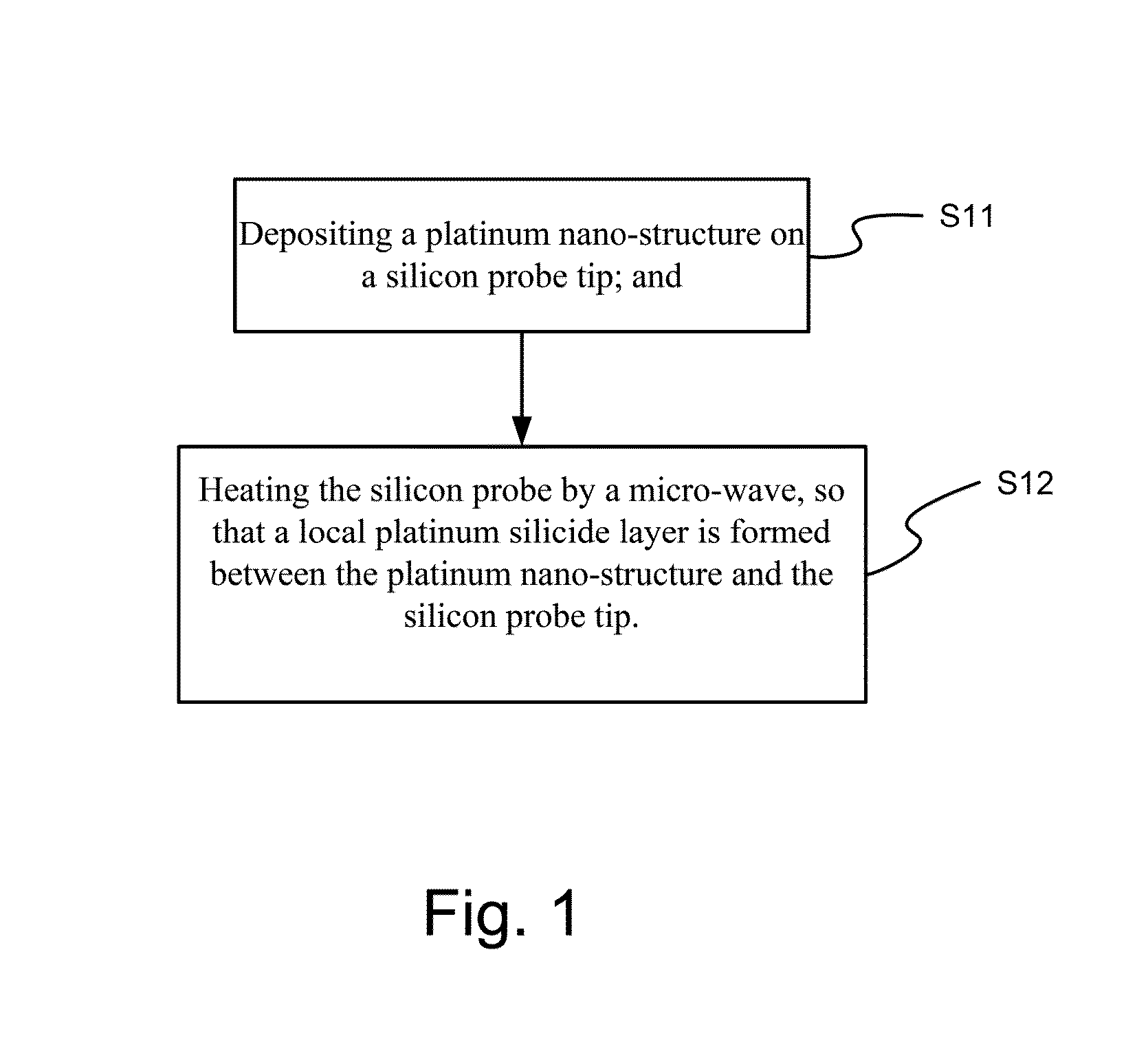
[0041]It is a main and the other objects of the present invention to provide a tip structure of a platinum-platinum silicide-silicon composite field sensor probe, and a method for forming a modified silicon tip apex (MSTA) structure on the probe, respectively, where a chemical deposition method is used in combination with a microwave annealing process so that a local platinum silicide layer is formed between a platinum nano-structure and a silicon probe tip with a good spatial resolution and sensitivity, which may largely enhance a tip conductivity and a field sensor spaciancel resolution.

[0042]According to the present invention, the tip structure of a platinum-platinum silicide-silicon composite field sensor probe comprises a silicon probe tip; a platinum nano-structure, growing on the silicon probe tip; and a local platinum silicide layer, disposed between the silicon probe tip and the platinum nano-structure to increase a tip field sensor resolution ability.

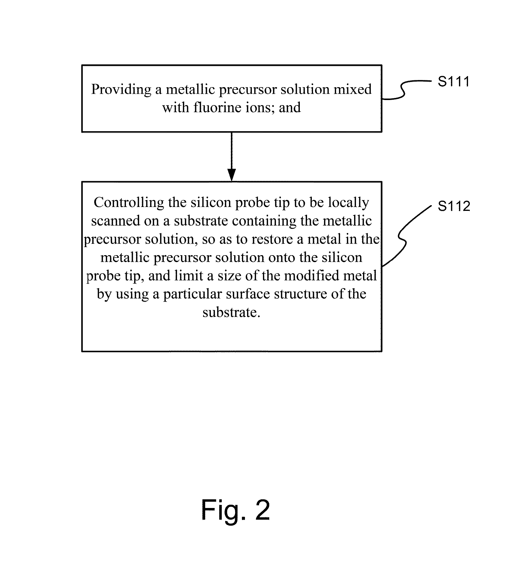
[0043]In an embodiment...


PUM

PropertyMeasurementUnit
poweraaaaaaaaaa
poweraaaaaaaaaa
particle diameteraaaaaaaaaa

Abstract

A platinum-platinum silicide modified silicon composite tip apex, and a method for forming the aforesaid tip apex are disclosed, where a metallic precursor solution and a silicon probe are reacted to form a local platinum nano-structure, which could be precisely controlled with local selectivity, and a local platinum silicide layer is formed between the platinum nano-structure and the silicon probe with an atmospheric microwave annealing (a-MWA) process conducted as well, largely enhancing the conductivity of the tip and spatial resolution of the field detection in field sensitive scanning probe microscopy. In addition to exemption from a stray-field effect and thus having better image quality, the platinum silicide-containing probe could more efficiently enhance the interfacial electron transfer efficiency as compared to the probe tip having only a platinum nano-structure, so that the probe could be applicable to a controlled conductive probe having high spatial resolution.

Description

FIELD OF THE INVENTION[0001]The present invention relates to a tip structure of a platinum-platinum silicide-silicon composite field sensor probe used for field detection, and a method for forming a modified silicon tip apex structure (MSTA) on the probe, and particularly to such structure and method where a chemical deposition process is combined with a microwave annealing process, so as to form a local platinum silicide layer between the platinum nano-structure and the silicon probe tip, and more particularly to such structure and method equipped with a good spatial resolution and sensitivity, which may largely enhancing a conductivity of the tip and a spatial resolution of the field detection.DESCRIPTION OF THE RELATED ART[0002]In study of material used for a tip, it is the first issue to focus on the measurement of the optical, electrical, magnetic and mechanical properties of the tip in a nano-level. The Field sensitive scanning probe microscopic technology (FS-SPM) may include...

Claims


Application Information

Patent Timeline
Patent Type & Authority Patents(United States)
IPC IPC(8): G01Q70/14G01Q70/18
CPCG01Q70/18G01Q70/14
Inventor LIN, CHUN-TINGSHIAO, MING-HUATUNG, SHU-HUNGCHANG, MAO-NAN
Owner NAT APPLIED RES LAB
Why Eureka
Try Eureka