Fast recovery diode and manufacturing method thereof

A recovery diode and manufacturing method technology, applied in the field of microelectronics, to achieve the effect of ensuring uniformity and solving the problem of uniformity of switching speed

Inactive Publication Date: 2010-11-10
商海涵
View PDF4 Cites 0 Cited by
  • Summary
  • Abstract
  • Description
  • Claims
  • Application Information

AI Technical Summary

Problems solved by technology

[0004] The technical problem to be solved by the present invention is to provide a fast recovery diode, which can solve the problem of DIE toDIE and WAFER to WAFER switching speed uniformity

Method used


Image

  • Fast recovery diode and manufacturing method thereof
  • Fast recovery diode and manufacturing method thereof
  • Fast recovery diode and manufacturing method thereof

Examples


Embodiment Construction

[0019] Embodiments of the present invention provide a fast recovery diode and a manufacturing method thereof, which can solve the problem of DIE-to-DIE and WAFER-to-WAFER switching speed uniformity.

[0020] The fast recovery diode of the embodiment of the present invention and its manufacturing method will be described in detail below with reference to the accompanying drawings.

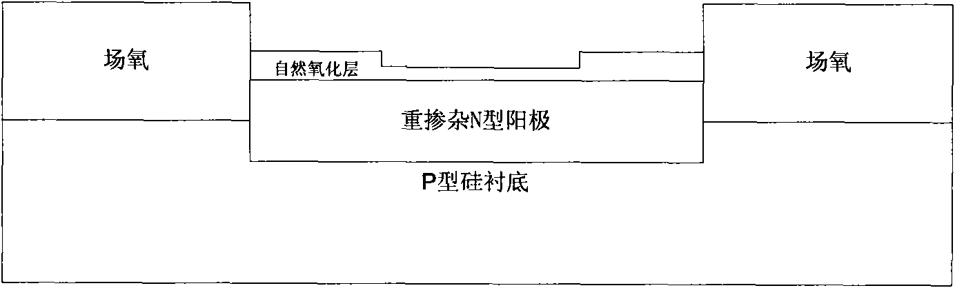
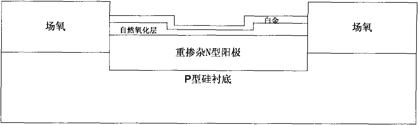
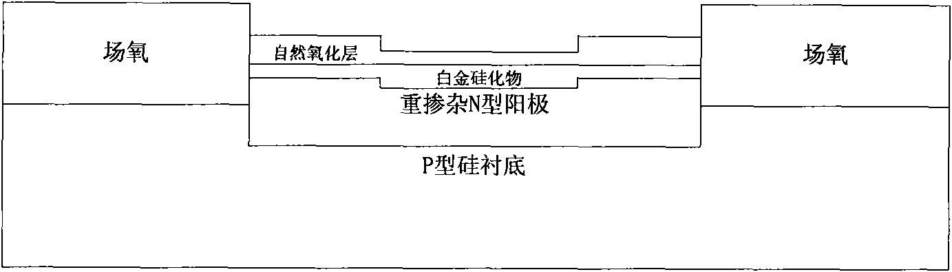
[0021] figure 2 It is a structural schematic diagram of an FRD embodiment of the present invention, such as figure 2 As shown, the fast recovery diode of the embodiment of the present invention includes: a silicon substrate, a heavily doped anode deposited on the silicon substrate, and field oxygen deposited on the silicon substrate and on both sides of the heavily doped anode, It also includes: a platinum silicide layer formed on the heavily doped anode and a uniform silicon dioxide layer formed on the platinum silicide layer.

[0022] In the fast recovery diode provided by the embodiment of th...


PUM


Abstract

The invention discloses a fast recovery diode and a manufacturing method thereof, relating to the field of micro-electronics, and solving the problem of speed uniformity of switching DIE to DIE and WAFER to WAFER of the fast recovery diode manufactured by the traditional technology. The fast recovery diode of the invention comprises a silicon substrate, a heavy doping anode, field oxide, a platinum silicide layer and an even silicon dioxide layer, wherein the heavy doping anode is deposited on the silicon substrate, the field oxide is deposited on the silicon substrate and is arranged on two sides of the heavy doping anode, the platinum silicide layer is formed on the heavy doping anode, and the even silicon dioxide layer is formed on the platinum silicide layer. The method comprises the following steps: forming the even silicide dioxide layer on the silicon substrate on which the heavy doping anode and the field oxide are deposited after the cleaning; depositing a metal layer with the sputtering or evaporating method; and by using the alloy technology, forming even silicide nodes. The invention is applied to manufacture of the fast recovery diode.

Description

technical field [0001] The invention relates to the field of microelectronics, in particular to a fast recovery diode and a manufacturing method thereof. Background technique [0002] Fast Recovery Diode (FRD for short) is a high-speed switching device that introduces deep-level metal impurities on the basis of ordinary diodes to form a resurrection center, thereby increasing the switching speed. Figure 1A-Figure 1C It is a schematic diagram of the manufacturing method of the prior art FRD, such as Figures 1A-1C As shown, firstly, a heavily doped N-type anode is formed on a P-type silicon substrate by a traditional process, and after the cleaning before metal deposition is completed, the metal is deposited directly, and in the time interval between the two steps, the silicon wafer A non-uniform natural oxide layer (silicon dioxide layer) will be formed rapidly on the surface, thereby affecting the uniformity of the metal silicide thickness, resulting in the ubiquity of chi...

Claims


Application Information

Patent Timeline
Patent Type & Authority Applications(China)
IPC IPC(8): H01L29/861H01L29/417H01L21/329H01L21/283
Inventor 商海涵
Owner 商海涵
Why Eureka
Try Eureka