

Self-aligned light angle sensor using thin metal silicide anodes
a technology of light angle sensor and metal silicide anode, which is applied in the direction of instruments, diagnostic recording/measuring, and using reradiation, etc., can solve the problems of difficult to reduce the size of the device, the use of lenses in these detectors has several limitations, and the matter of timely and costly matters
Active Publication Date: 2021-09-23
ANALOG DEVICES INC
View PDF3 Cites 0 Cited by
- Summary
- Abstract
- Description
- Claims
- Application Information
AI Technical Summary
Benefits of technology
This patent describes a new method for detecting objects in space at precise angles using optical detection. The method involves designing and fabricating special photodiode arrays that can measure the angle of incident light in multiple dimensions. The design uses self-aligned Schottky platinum silicide PIN photodiodes, which guarantees accurate measurements without any offset errors. The manufacturing process is also simplified compared to traditional designs. The technical effects of this patent are improved accuracy and efficiency in optical detection, with reduced device offset errors and simplified manufacturing process.
Problems solved by technology
This can become a timely and costly matter.
While lenses were needed to focus the light on a particular area of the detector in order to measure the properties of the light emitted from a light source, the use of lenses in these detectors has several limitations.
This required separation between the lens and the light detecting surface consumes extra space in electronic devices, which makes it difficult to reduce the size of the device.
Second, the lenses also represent a cost component of a detector.
However, the trench reduced the light collection efficiency of these photodetectors because the light passing through the aperture that reaches the trench would not be detected by the photodetectors.
Additionally, trenches have been difficult to manufacture on germanium based epitaxial layers, which provide improved light detection capabilities over silicon based epitaxial layers.
Method used
View moreImage
Smart ImageViewing Examples

Examples
example 13
[0211 provides a method according to example 10 wherein the blocking member comprises a very thin layer of metal.
example 14
[0212 provides a method according to example 10 wherein the intrinsic layer comprises undoped silicon.
example 15
[0213 provides a method according to example 10 further comprising depositing an optical filter.
Login to View More PUM
| Property | Measurement | Unit |
|---|---|---|
| heights | aaaaa | aaaaa |
| heights | aaaaa | aaaaa |
| outer diverging angle | aaaaa | aaaaa |
Abstract
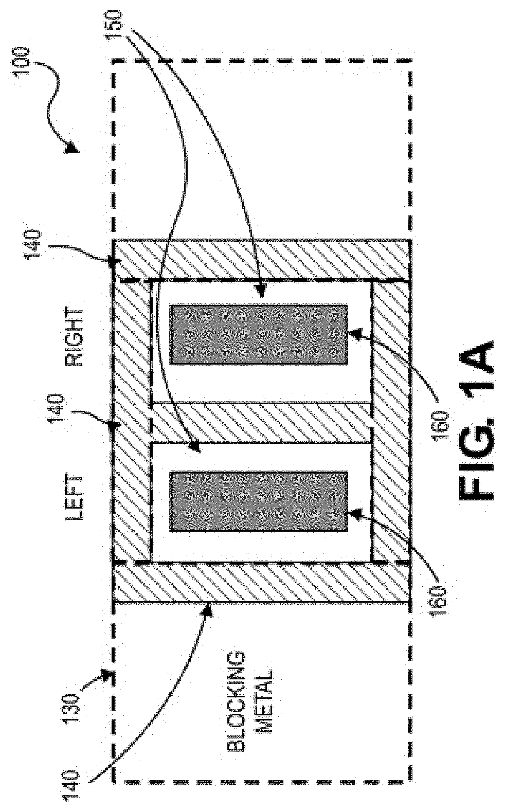
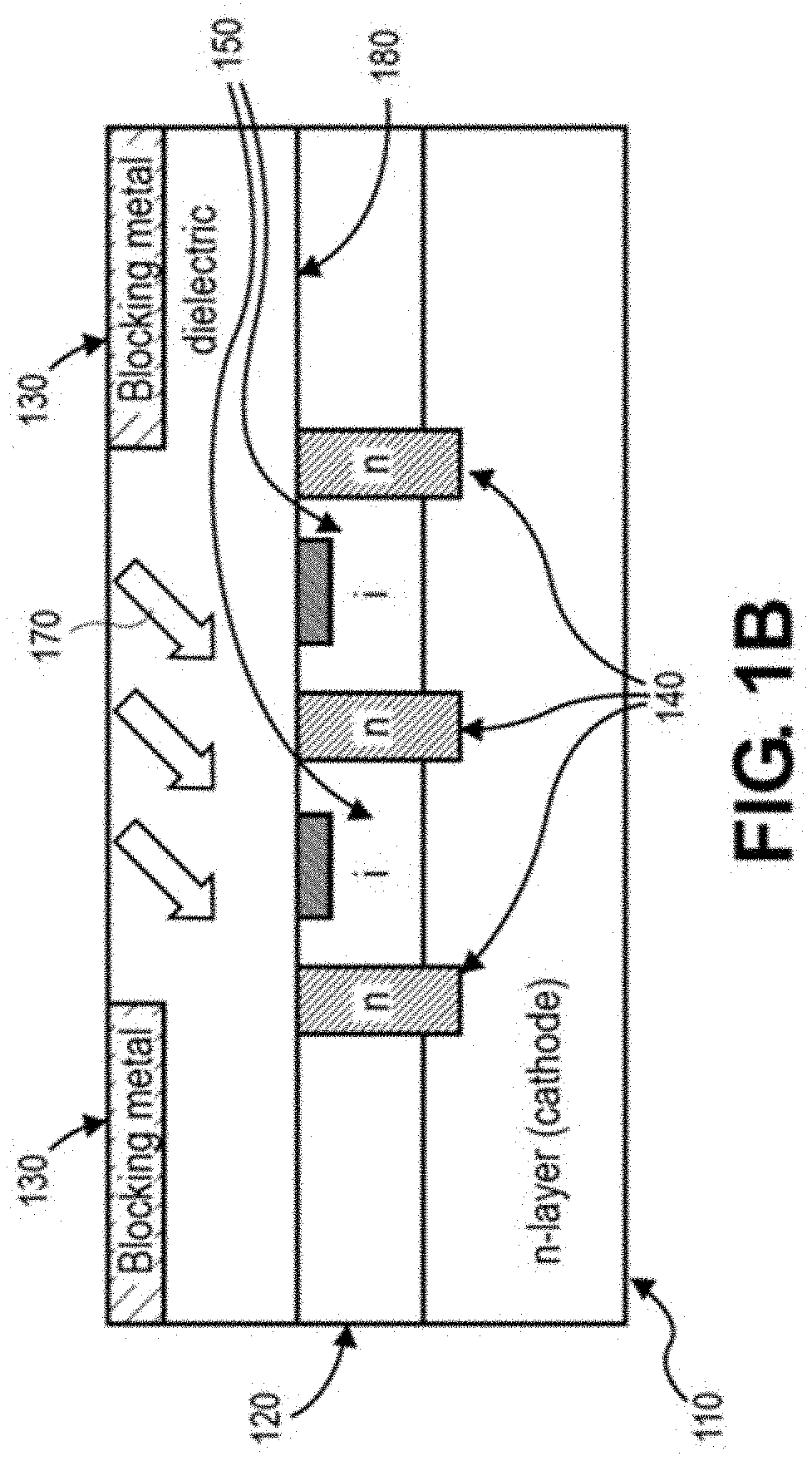
Aspects of the embodiments are directed to non-contact systems, methods and devices for optical detection of objects in space at precise angles. This method involves the design and fabrication of photodiode arrays for measuring angular response using self-aligned Schottky platinum silicide (PtSi) PIN photodiodes (PN-diodes with an intrinsic layer sandwiched in between) that provide linear angular measurements from incident light in multiple dimensions. A self-aligned device is defined as one in which is not sensitive to photomask layer registrations. This design eliminates device offset between “left” and right” channels for normal incident light as compared to more conventional PIN diode constructions.
Description
CROSS-REFERENCE TO RELATED APPLICATIONS[0001]This application is related to U.S. Utility patent application Ser. No. 13 / 924,797 entitled, “OPTICAL ANGLE MEASUREMENT” filed on Jun. 24, 2013, currently granted U.S. Pat. No. 9,435,641, and to U.S. Utility patent application Ser. No. 13 / 329,510 entitled, “LENS-LESS OPTICAL POSITION MEASURING SENSOR” filed on Dec. 19, 2011, currently granted U.S. Pat. No. 9,702,690, both of which are hereby incorporated by reference in their entirety.FIELD OF THE DISCLOSURE[0002]The present disclosure relates to a self-aligned light angle sensor. More specifically, this disclosure describes apparatus and methods relating to fabricating self-aligned light angle sensors using thin metal silicide anodes and applications thereto.BACKGROUND[0003]Light angle sensors are used in a variety of applications, for example, gesture for user interface control in portable devices, object location tracking, industrial and automation monitoring, angle sensing, proximity ...
Claims
Login to View More Application Information
Patent Timeline
 Patent Type & AuthorityApplications(United States)
IPC IPC(8): G01B11/27H01L29/872H01L29/66
CPCG01B11/272H01L29/66143H01L29/872G01B11/26H01L31/02164H01L31/102H01L31/105H01L31/108H01L31/022408H01L31/028H01L31/03044H01L27/1446H01L31/02024G01S7/4816G01S17/48A61B5/14552A61B2562/0233G01S3/7835G01S3/781Y02P70/50
InventorDELIWALA, SHRENIKSTEVENS, PAUL W.O'MARA, WILLIAM EDWARD
OwnerANALOG DEVICES INC