Semiconductor device, three-dimensional semiconductor device, and method of manufacturing semiconductor device

a semiconductor device and semiconductor technology, applied in semiconductor devices, semiconductor/solid-state device details, electrical apparatus, etc., can solve the problems of difficult to form through holes, difficulty in wire bonding and connecting with other electrodes, and increase in connection resistan

Inactive Publication Date: 2005-08-04
FUJITSU LTD
View PDF4 Cites 114 Cited by
  • Summary
  • Abstract
  • Description
  • Claims
  • Application Information

AI Technical Summary

Benefits of technology

[0027] In accordance with the present invention, a semiconductor device that is thinner than the original crystals of a semiconductor substrate obtained by slicing single-crystalline ingot can be manufactured. As the lead-out unit is formed after the semiconductor substrate is thinned, the formation of the hole in the semiconductor substrate can be carried out in a short period of time.

Problems solved by technology

As a result, an increase in the connection resistance cannot be avoided between each electrode pad and the corresponding via wiring plug.
Also, having a through electrode in the middle, each of the electrode pads has a smaller area, resulting in difficulties in wire bonding and connecting with other electrodes.
Therefore, it is difficult to form the through holes, while maintaining the flatness of each semiconductor chip.
Therefore, it is difficult to form an insulating layer and a conductive layer with sufficient thicknesses in each through hole.
As a result, each semiconductor chip takes up a large area.
Therefore, this structure is not suitable for high integration.
In accordance with this prior art, it is difficult to produce a small-sized memory three-dimensional semiconductor device.

Method used


Image

  • Semiconductor device, three-dimensional semiconductor device, and method of manufacturing semiconductor device
  • Semiconductor device, three-dimensional semiconductor device, and method of manufacturing semiconductor device
  • Semiconductor device, three-dimensional semiconductor device, and method of manufacturing semiconductor device

Examples


first embodiment

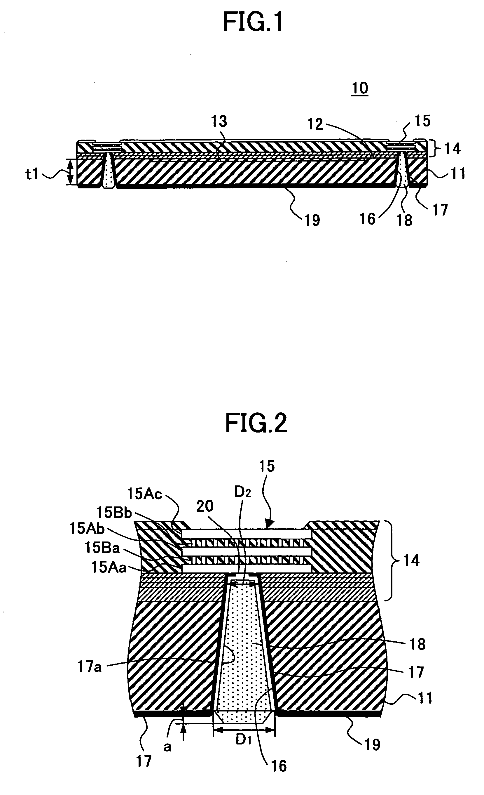
[0083]FIG. 1 illustrates the structure of a semiconductor device in accordance with a first embodiment of the present invention. FIG. 2 is a partially enlarged cross-sectional view of the semiconductor device.

[0084] The semiconductor device 10 shown in FIG. 1 has an electronic circuit unit (an integrated circuit unit) 13 that includes an active element, a passive element, and an electrode / wiring layer. The electronic circuit unit 13 is formed on a principal surface of a thin silicon semiconductor substrate 11. The wiring layer lead out from the electronic circuit unit 13 extends in an insulating layer, and is electrically connected to an electrode pad 15.

[0085] The semiconductor substrate 11 has a hole 16 formed at the location corresponding to the electrode pad 15. This hole 16 does not penetrate the electrode pad 15.

[0086] An embedded electrode 18 is provided in the hole 16 via an insulating layer 17 and a base (seed) metal layer 17a. The insulating layer 17 is formed to cover ...

second embodiment

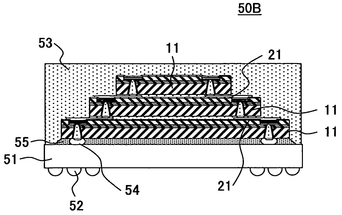
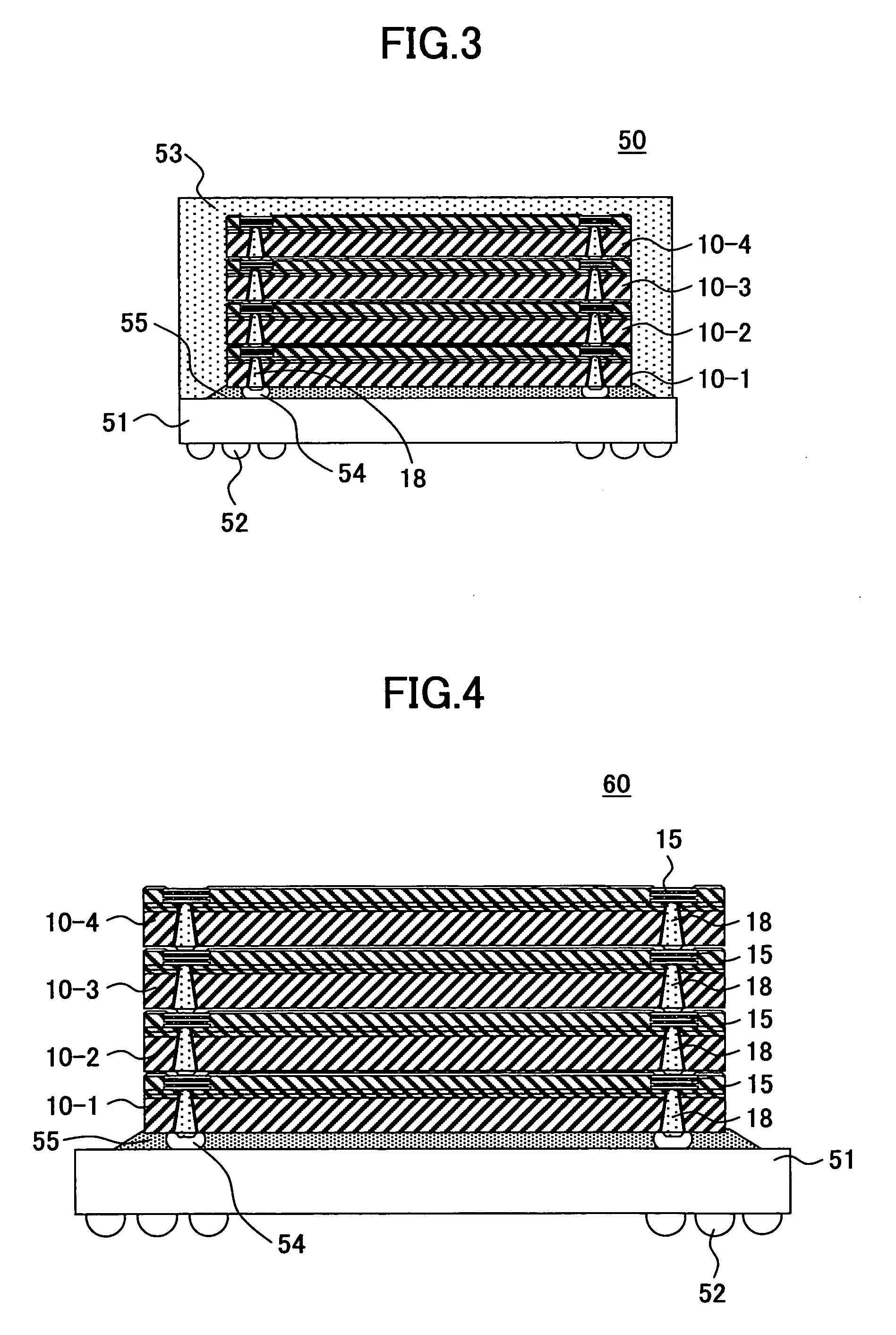
[0109]FIG. 3 illustrates the structure of a three-dimensional semiconductor device 50 as a second embodiment of the present invention. This three-dimensional semiconductor device 50 is formed with the semiconductor device 10 with the above described structure in accordance with the present invention.

[0110]FIG. 4 is an enlarged cross-sectional view of the substantial part of the semiconductor device 50, which is a semiconductor device laminated body.

[0111] In accordance with this embodiment, the semiconductor device 50 has an insulating resin sheet as a base member, and a supporting substrate (an interposer) 51 that has an electrode / wiring layer formed on the surface and / or in the inside thereof. A plural number (four (10-1 through 10-4) in FIGS. 3 and 4) of semiconductor devices 10 of the first embodiment are laminated and mounted on a principal surface of the supporting substrate 51. An external connection terminal 52 is provided on the other principal surface of the supporting s...

third embodiment

[0121]FIG. 5 illustrates a third embodiment of the present invention. The third embodiment is a modification of the three-dimensional semiconductor device having the semiconductor devices 10 in accordance with the present invention.

[0122] In this embodiment, a semiconductor device 50A has an insulating resin sheet as a base member, and a supporting substrate (an interposer) 61 that has an electrode / wiring layer formed on the surface and / or in the inside thereof. A plural number (four (10-1 through 10-4) in FIG. 5) of semiconductor devices 10 of the first embodiment are laminated and mounted on a principal surface of the supporting substrate 61. An external connection terminal 62 is provided on the other principal surface of the supporting substrate 61.

[0123] The laminated body of the semiconductor devices 10 is packaged and sealed with epoxy resin 63.

[0124] In FIG. 5, reference numeral 64 indicates a solder bump, and reference numeral 65 indicates an underfill that is made of res...


PUM


Abstract

A semiconductor device is provided that forms a three-dimensional semiconductor device having semiconductor devices stacked on one another. In this semiconductor device, a hole is formed in a silicon semiconductor substrate that has an integrated circuit unit and an electrode pad formed on a principal surface on the outer side. The hole is formed by etching, with the electrode pad serving as an etching stopper layer. An embedded electrode is formed in the hole. This embedded electrode serves to electrically lead the electrode pad to the principal surface on the bottom side of the silicon semiconductor substrate.

Description

CROSS-REFERENCE TO RELATED APPLICATION [0001] This application is a U.S. continuation application filed under 35 USC 111(a) claiming benefit under 35 USC 120 and 365(c) of PCT International Application No. PCT / JP03 / 00283 filed on Jan. 15, 2003, which is hereby incorporated herein by reference.BACKGROUND OF THE INVENTION [0002] The present invention generally relates to semiconductor devices, three-dimensional semiconductor devices, and methods of manufacturing semiconductor devices, and, more particularly, to a semiconductor device that is suitable for a stacked structure, a three-dimensional semiconductor device that is formed by stacking the semiconductor devices on one another, and a method of manufacturing the semiconductor device. [0003] In recent years, three-dimensional semiconductor devices in which semiconductor devices are stacked on one another have been developed as highly-integrated, smaller semiconductor components. To produce a three-dimensional semiconductor device w...

Claims


Application Information

Patent Timeline
Patent Type & Authority Applications(United States)
IPC IPC(8): H01L21/768H01L23/31H01L23/48H01L23/485H01L23/522H01L25/065H01L29/76
CPCH01L21/76898H01L23/3128H01L2924/0002H01L2224/16225H01L2224/05572H01L2224/13025H01L2224/06181H01L23/481H01L25/0657H01L25/50H01L2224/0401H01L2224/16145H01L2225/06513H01L2225/06517H01L2225/06524H01L2225/06527H01L2225/06541H01L2225/06551H01L2225/06555H01L2924/01002H01L2924/01004H01L2924/01005H01L2924/01006H01L2924/01011H01L2924/01013H01L2924/01014H01L2924/01015H01L2924/01022H01L2924/01027H01L2924/01028H01L2924/01029H01L2924/01039H01L2924/01047H01L2924/0106H01L2924/01074H01L2924/01075H01L2924/01078H01L2924/01079H01L2924/01082H01L2924/014H01L2924/05042H01L2924/14H01L2924/15311H01L2924/01019H01L2924/01033H01L2224/02371H01L2224/13008H01L24/05H01L24/13H01L24/16H01L2224/131H01L2224/16227H01L2924/00012H01L2224/05552H01L2224/13009H01L2224/45144H01L2924/12042H01L2924/181
Inventor YOSHIDA, EIJIOHNO, TAKAOAKUTAGAWA, YOSHITOSAWAHATA, KOJIMIZUKOSHI, MASATAKANISHIMURA, TAKAOTAKASHIMA, AKIRAWATANABE, MITSUHISA
Owner FUJITSU LTD
Why Eureka
Try Eureka