Apparatus and method for processing wafers

a technology of apparatus and wafers, applied in the field of apparatus and processing wafers, can solve the problems of time-consuming and separate process, no commercially available system permits parallel processing of a plurality, etc., and achieves the effects of reducing the number of positioning and movement steps, improving the reliability of laser fuses, and improving the reliability of processing

Inactive Publication Date: 2005-08-04
POLARIS INNOVATIONS
View PDF13 Cites 24 Cited by
  • Summary
  • Abstract
  • Description
  • Claims
  • Application Information

AI Technical Summary

Benefits of technology

[0011] The present invention provides a system which minimizes many of the positioning and movement s...

Problems solved by technology

The beam positioning process is thus unique for each wafer and, as a result, in addition to finding the alignment marks complex and very time-consuming, none of the commercially available systems permits parallel processing of a plural...

Method used


Image

  • Apparatus and method for processing wafers
  • Apparatus and method for processing wafers
  • Apparatus and method for processing wafers

Examples


Embodiment Construction

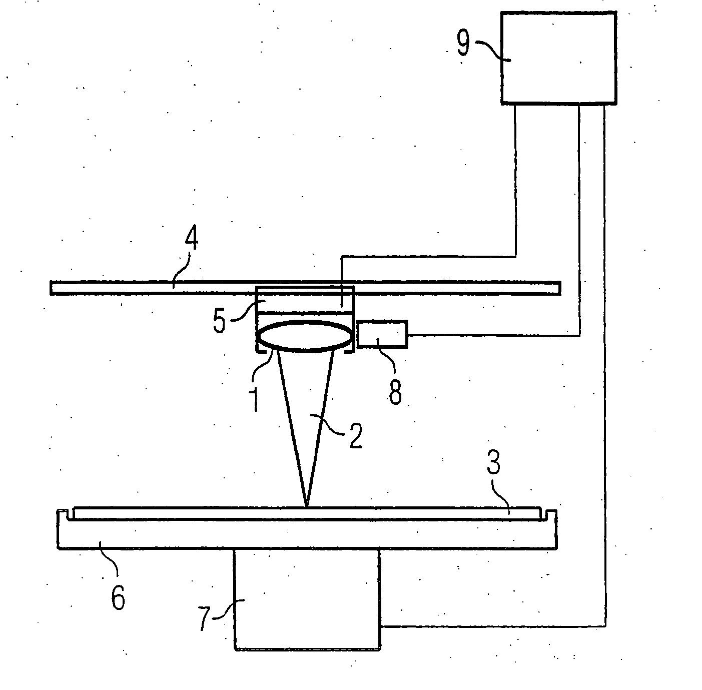
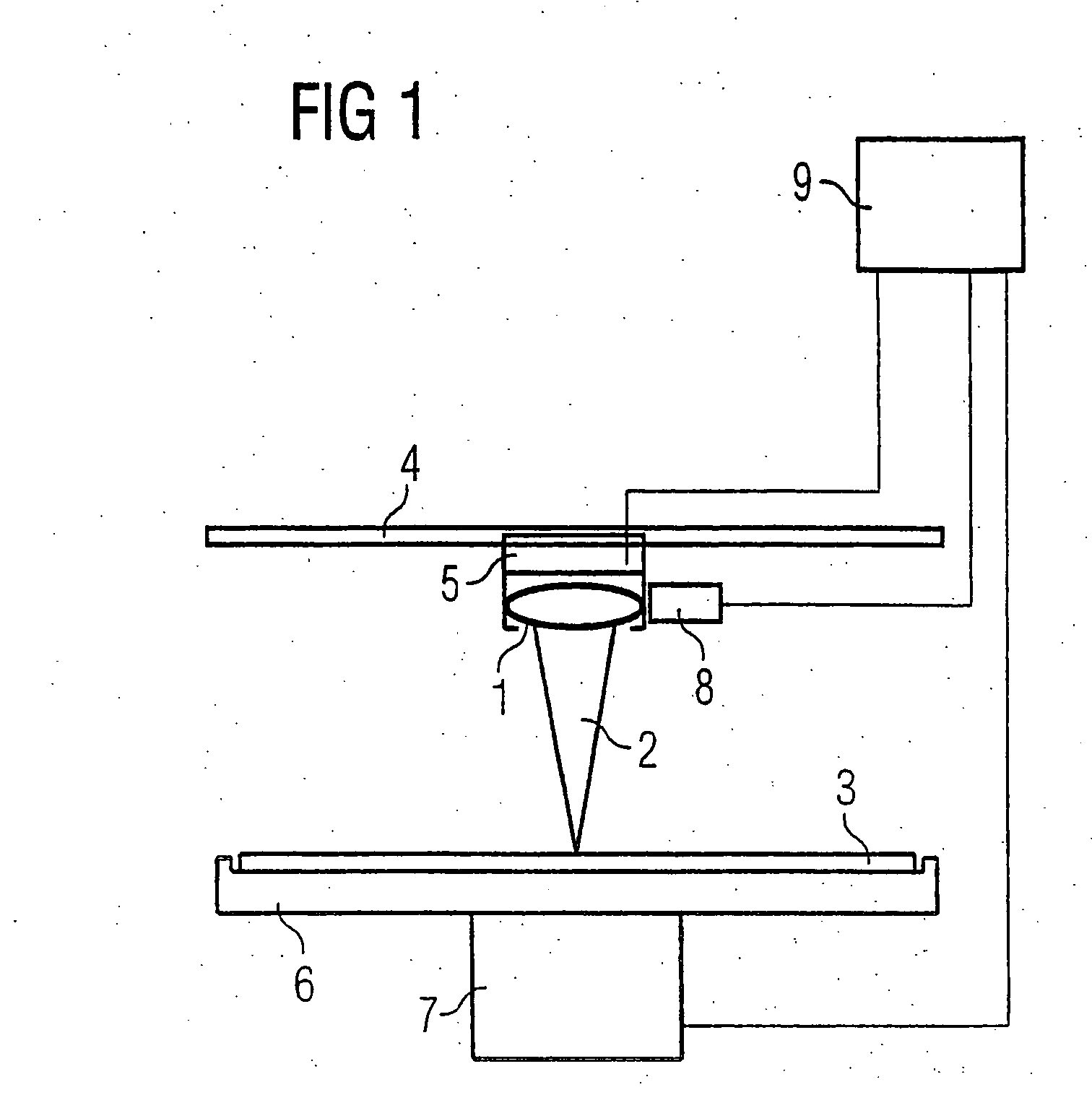
[0039]FIG. 1 schematically shows a processing apparatus 1, employing a processing tool, such as a laser beam 2 focused onto a wafer 3. The processing apparatus 1 moves in the radial direction over the wafer, for example with the aid of a linear motor 5 guided at a rail 4. Alternate mechanisms are also possible, for example a galvanometric system in which the laser focus can be guided over the wafer by means of mirrors without necessitating a mechanical movement of the processing apparatus 1. A wafer support 6 and an associated positioning system 7 serve for rotation and positioning of the wafer 3. A position determining apparatus 8 is arranged at the processing apparatus 1 and is connected to a control apparatus 9 via a cable. Further cables are connected to the positioning systems 5 and 7 and serve for driving the motors for the positioning of wafer 3 and processing apparatus 1.

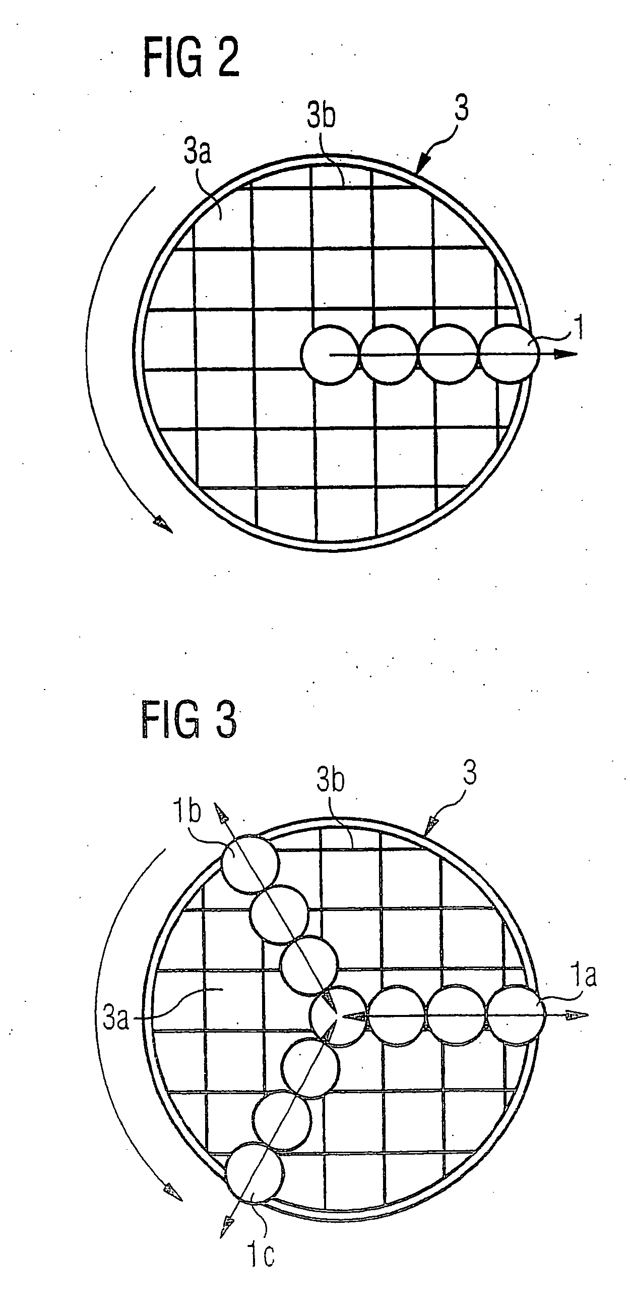
[0040]FIG. 2 shows a first embodiment of the present invention in planar view. The wafer 3, with a serie...


PUM


Abstract

An apparatus for processing semiconductor wafers includes: a wafer support with a first positioning system that can rotate the wafer support coaxially with a wafer; at least one processing apparatus, which can be moved with a second positioning system such that a processing tool proceeding from the processing apparatus can be guided radially over the wafer; and at least one position determining apparatus for determining a wafer position on the basis of features of the wafer. Alignment marks of the wafer are found and points to be processed, such as laser fuses, are moved by rotation of the wafer and movement of at least one processing apparatus in the radial direction above the wafer.

Description

CROSS REFERENCE TO RELATED APPLICATIONS [0001] This application is a continuation of PCT / DE2003 / 02554, filed Jul. 30, 2003, and titled “Processing Device for Wafers and Method for Processing Thereof,” which claims priority to German Application No. DE 1023493.6, filed on Jul. 31, 2002, and titled “Processing Device for Wafers and Method for Processing Thereof,” the entire contents of which are hereby incorporated by reference. FIELD OF THE INVENTION [0002] At the present time so-called “laser fuses” are used on many semiconductor chips. They are wirelike semiconductor structures on the chips which can be destroyed and then electrically opened by means of a laser beam. The fuses, which are referred to as “links”, are used to repair memory chips, to program specific functions, to set operating voltages and frequencies and to provide chips with specific identification features. In the case of expensive semiconductor chips, reserve areas comprising structures are provided. Occasionally,...

Claims


Application Information

Patent Timeline
IPC IPC(8): H01L21/68
CPCH01L21/68
Inventor KEMPER, FRANZMOCKEL, JENS
Owner POLARIS INNOVATIONS
Why Eureka
Try Eureka