Method of manufacturing a semiconductor device including electrodes on main and reverse sides of a semiconductor chip

Inactive Publication Date: 2005-08-04
DENSO CORP
View PDF12 Cites 22 Cited by
  • Summary
  • Abstract
  • Description
  • Claims
  • Application Information

AI Technical Summary

Benefits of technology

[0041] Furthermore, by covering the edge face of the semiconductor wafer and the edge face of the first resin with the second resin having acid resistance and alkaline r

Problems solved by technology

The warpage of this kind may cause a breakage of the semiconductor wafer.
The warpage also causes a proble

Method used


Image

  • Method of manufacturing a semiconductor device including electrodes on main and reverse sides of a semiconductor chip
  • Method of manufacturing a semiconductor device including electrodes on main and reverse sides of a semiconductor chip
  • Method of manufacturing a semiconductor device including electrodes on main and reverse sides of a semiconductor chip

Examples


Embodiment Construction

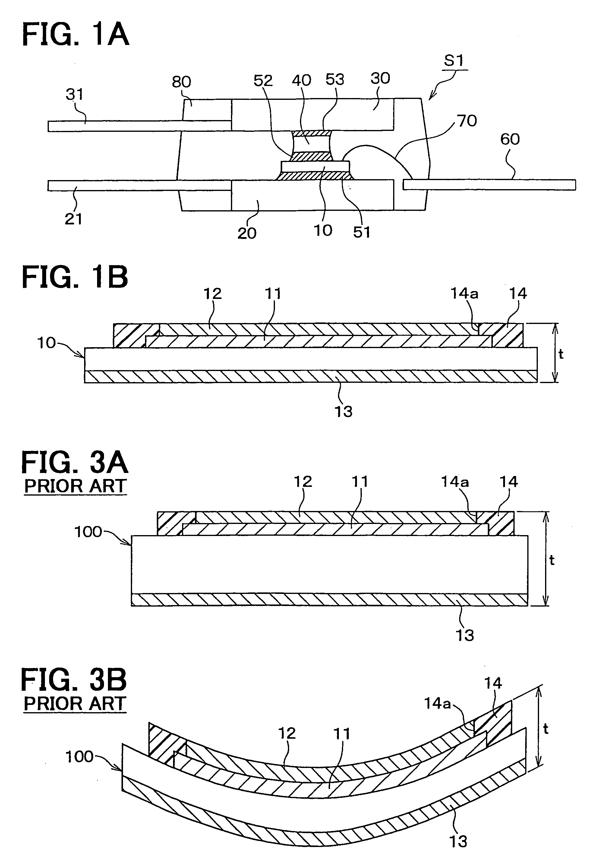
[0047] A preferred embodiment will be described with reference to the drawings. In each of the drawings, the same or equivalent portions have the same numerals for the purpose of simplicity of description.

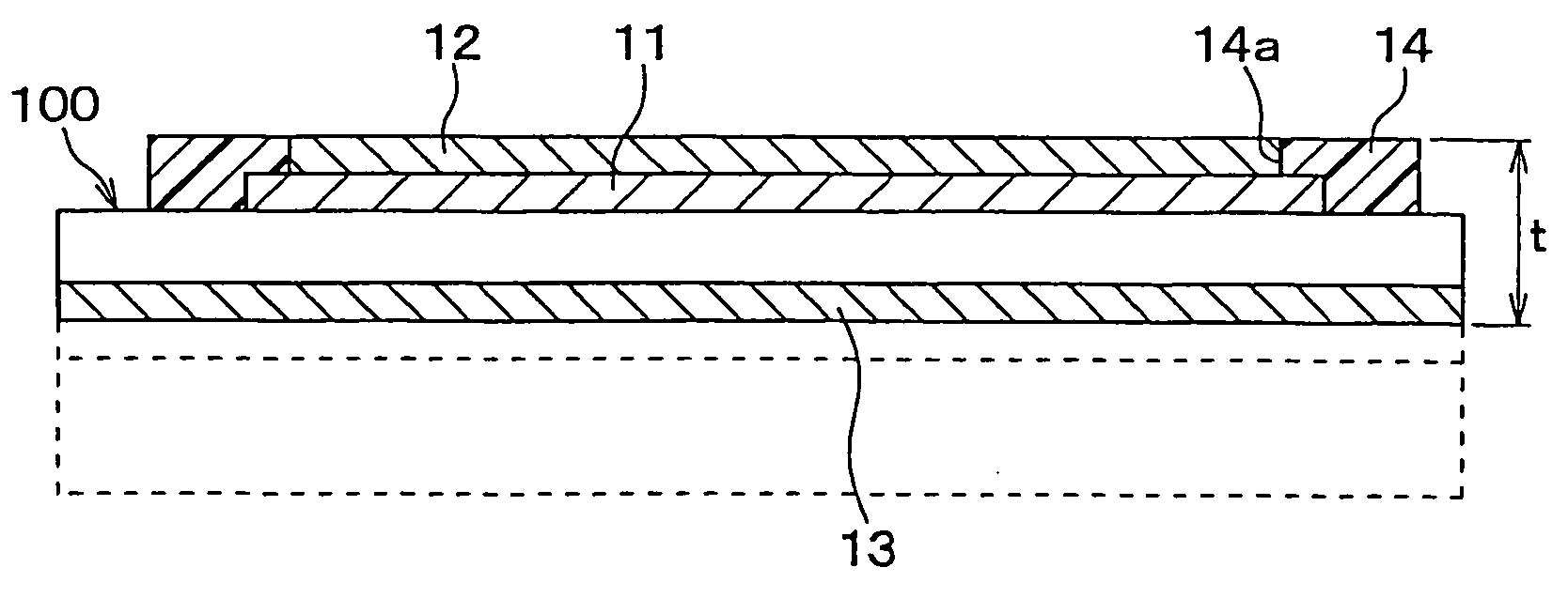
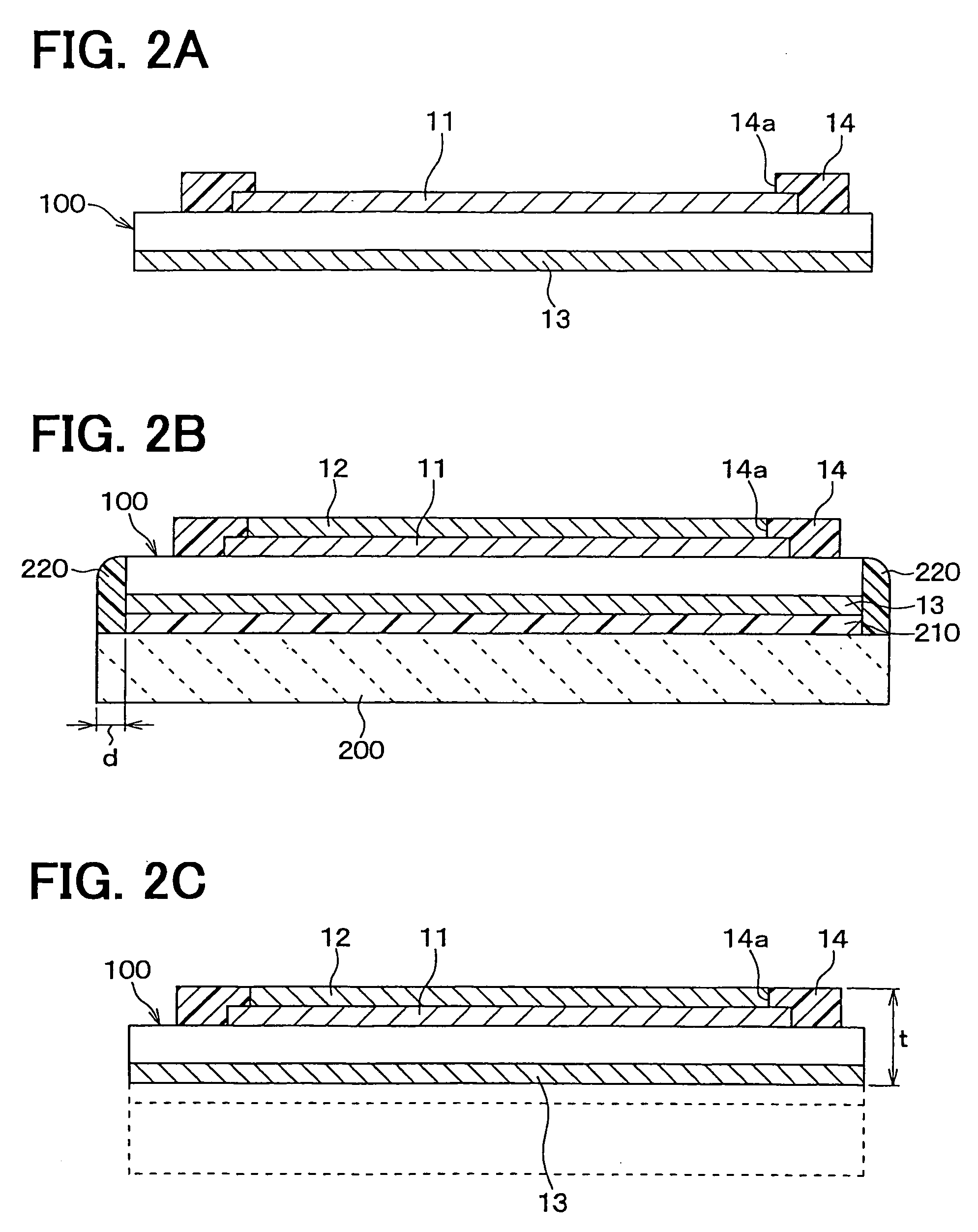
[0048] As shown in FIG. 1A, the semiconductor device Si includes a semiconductor chip 10, a lower heatsink 20 as a first metal body, an upper heatsink 30 as a second metal body 30, a heatsink block 40, conductive adhesives 51, 52, 53 interposing between the chip and the heatsinks, and a resin mold 80.

[0049] In this structure, a lower side of the semiconductor chip 10 and an upper side of the lower heatsink 20 are connected by the first conductive adhesive 51.

[0050] Further, an upper side of the semiconductor chip 10 and a lower side of the heatsink block 40 are connected by the second conductive adhesive 52.

[0051] Furthermore, an upper side of the heatsink block 40 and a lower side of the upper heatsink 30 are connected with the third conductive adhesive 53.

[0052] A solder, a ...


PUM


Abstract

A method for manufacturing a semiconductor chip includes preparing a semiconductor wafer to be oriented so that a main side and reverse side of the semiconductor wafer is oriented similar to a main side and reverse side of the semiconductor chip intended to be cut from the semiconductor wafer. An electrode is formed on a reverse side of the semiconductor wafer. Another electrode is formed on the main side of the semiconductor wafer while the reverse side of the wafer is fixed to a supporting substrate. The semiconductor wafer is cut later to form the semiconductor chip.

Description

CROSS REFERENCE TO RELATED APPLICATIONS [0001] This application is based upon, claims the benefit of priority of, and incorporates by reference the contents of, Japanese Patent Application No. 2004-20073 filed on Jan. 28, 2004 and Japanese Patent Application No. 2004-291396 filed on Oct. 4, 2004 FIELD OF THE INVENTION [0002] The present invention relates generally to a method of manufacturing a semiconductor chip for a semiconductor device, and, more particularly, to such a chip having electrodes on main and reverse sides, and metal bodies as electrodes and radiators. BACKGROUND OF THE INVENTION [0003] A conventional semiconductor chip includes an electrode formed on a main side and reverse side of the chip. The semiconductor chip may be a power element such as, for example, an IGBT (Insulated Gate Bipolar Transistor). [0004] The semiconductor chip of the IGBT or the like is then bound by a metal body such as a heatsink or the like, and almost entirely molded with resin to thereby e...

Claims


Application Information

Patent Timeline
IPC IPC(8): H01L21/28H01L21/44H01L21/4763H01L21/50H01L21/56H01L21/60H01L21/768H01L21/78H01L23/12H01L23/29H01L29/739
CPCH01L21/76838H01L2224/48091H01L2924/1305H01L2924/13055H01L2924/1301H01L2224/73265H01L2224/48247H01L2924/00014H01L2924/00
Inventor HIRANO, NAOHIKOMIURA, SHOJINIIMI, AKIHIRO
Owner DENSO CORP
Why Eureka
Try Eureka