Field emission device and backlight device using the field emission device and method of manufacture thereof

a field emission device and backlight technology, applied in lighting and heating apparatus, applications, instruments, etc., can solve the problems of ldcs themselves not being able to emit light to form images, consuming little electric power, and unable to observe images in a dark place, so as to enhance cnt growth

Inactive Publication Date: 2005-08-11
SAMSUNG SDI CO LTD
View PDF6 Cites 17 Cited by
  • Summary
  • Abstract
  • Description
  • Claims
  • Application Information

AI Technical Summary

Benefits of technology

[0024] According to still another aspect of the present invention, a method of manufacturing a field emission type backlight device is provided, the method comprising: arranging a top substrate and a bottom substrate in parallel and spaced apart from each other by a predetermined distance; arranging an anode electrode on the top substrate; arranging a fluorescent layer on the anode electrode, the fluorescent layer having a predetermined thickness; arranging a cathode electrode and a gate electrode in alternating parallel strips on the bottom substrate; arranging a catalytic metal layer on the cathode electrode to enhance CNT growth; and growing CNTs on the catalytic metal layer.

Problems solved by technology

The LCDs are light in weight and consume little electric power.
However, LDCs themselves cannot emit light to form images.
Thus, it is impossible to observe the images in a dark place.
However, in general, such backlight devices have a complicated construction, thereby being quite expensive.
Furthermore, light sources are disposed in the lateral sides of the backlight devices and thus, due to the reflection and transmission of light, consumption of electrical power increases.
Especially, as LCDs become larger, it becomes more difficult to ensure uniform brightness of a backlight device.
However, the density of the CNT emitters produced by the screen printing method is low, thereby causing a problem in obtaining a field emission device having a high brightness.
Moreover, the field emission device having the layered structure noted above needs repetitive patterning, which results in high production costs.

Method used


Image

  • Field emission device and backlight device using the field emission device and method of manufacture thereof
  • Field emission device and backlight device using the field emission device and method of manufacture thereof
  • Field emission device and backlight device using the field emission device and method of manufacture thereof

Examples


Embodiment Construction

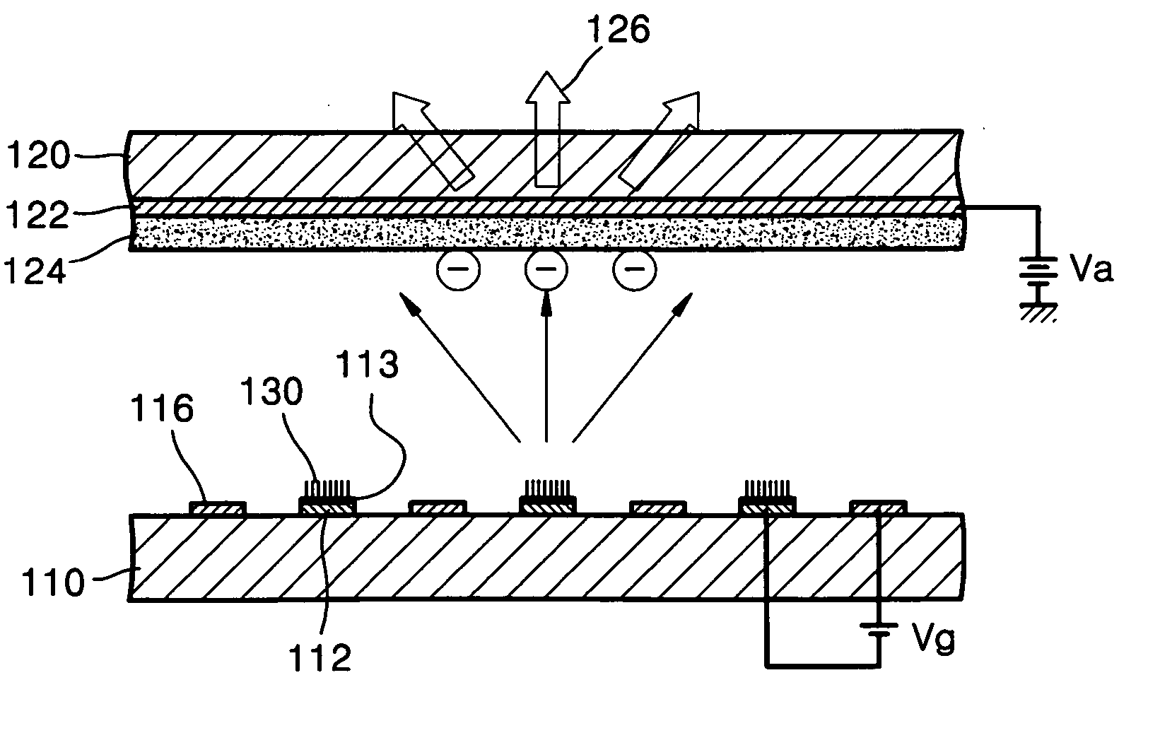
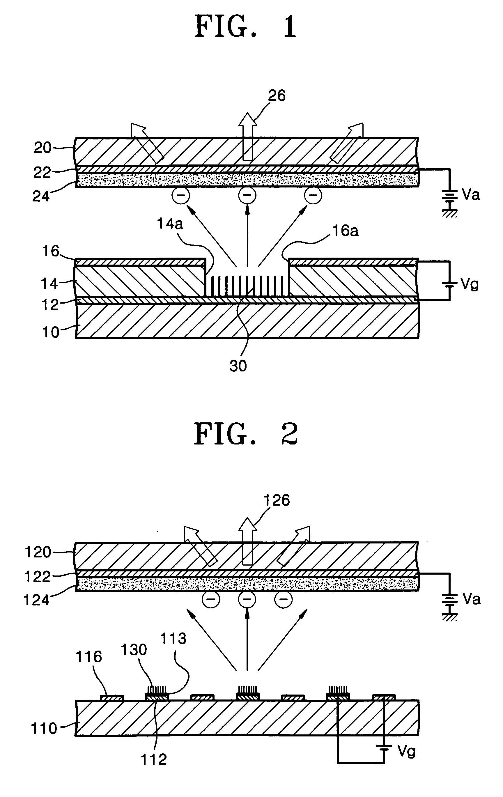
[0033]FIG. 1 is a partial cross-sectional view of a field emission type backlight device.

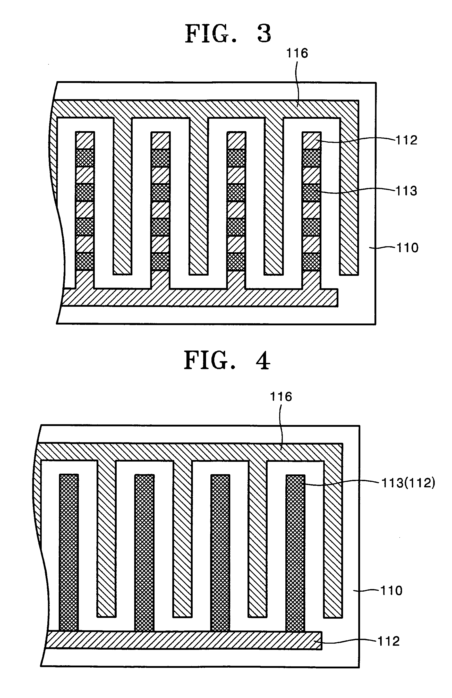
[0034] Referring to FIG. 1, a top substrate 20 and a bottom substrate 10 are disposed opposite to each other and spaced apart from each other by a predetermined distance. An anode electrode 22 and a fluorescent layer 24 are sequentially formed on an inner surface of the top substrate 20. A cathode electrode 12 is formed on an upper surface of the bottom substrate 10. A gate insulating layer 14 having a through hole 14a is formed on the cathode electrode 12. A gate electrode 16 is formed on the gate insulating layer 14, and the gate electrode 16 has a gate hole 16a corresponding to the through hole 14a. CNT emitters 30 are formed on an exposed surface of the cathode electrode 12 through the through hole 14a.

[0035] For the field emission type backlight device having the above structure, when a voltage Va of several kilovolts is supplied to the anode electrode 22 and a voltage Vg of several tens ...


PUM

PropertyMeasurementUnit
voltage Vgaaaaaaaaaa
thicknessaaaaaaaaaa
temperatureaaaaaaaaaa

Abstract

A field emission device and a backlight device using the field emission device includes a cathode electrode and a gate electrode formed in alternating parallel strips on a substrate, a catalytic metal layer arranged on the cathode electrode and adapted to enhance Carbon NanoTube (CNT) growth, and grown CNTs arranged on the catalytic metal layer.

Description

CLAIM OF PRIORITY [0001] This application makes reference to, incorporates the same herein, and claims all benefits accruing under 35 U.S.C. §119 from an application for FIELD EMISSION DEVICE AND BACKLIGHT DEVICE USING THE SAME earlier filed in the Korean Intellectual Property Office on 9 Feb. 2004 and there duly assigned Serial No. 10-2004-0008341. BACKGROUND OF THE INVENTION [0002] 1. Field of the Invention [0003] The present invention relates to a field emission device and a backlight device using the field emission device and a method of manufacture thereof, and more particularly, to a field emission device employing Carbon NanoTubes (CNTs) and a backlight device using the field emission device and a method of manufacture thereof. [0004] 2. Description of the Related Art [0005] In general, flat panel displays are roughly classified into light emitting displays and light receiving displays. The light emitting type displays include Cathode Ray Tubes (CRTs), plasma display panels (...

Claims


Application Information

Patent Timeline
Patent Type & Authority Applications(United States)
IPC IPC(8): G02F1/13357F21S2/00F21Y105/00H01J1/304H01J3/02H01J29/48H01J63/06
CPCB82Y10/00H01J1/304H01J2201/30469H01J29/481H01J63/06H01J3/022A01K87/007G01B3/10
Inventor JUNG, JAE-EUNKIM, JONG-MINOH, TAE-SIKPARK, YOUNG-JUN
Owner SAMSUNG SDI CO LTD
Why Eureka
Try Eureka