

Method of forming a shallow trench-deep trench isolation region for a BiCMOS/CMOS technology
a technology of bicmos/cmos and isolation region, which is applied in the manufacture of semiconductor/solid-state devices, basic electric elements, electric devices, etc., can solve the problems of unwanted topographies, leakage or shortening between intended devices, and achieve the effect of reducing the complexity of defining
- Summary
- Abstract
- Description
- Claims
- Application Information
AI Technical Summary
Problems solved by technology
Method used
Image

Examples
Embodiment Construction
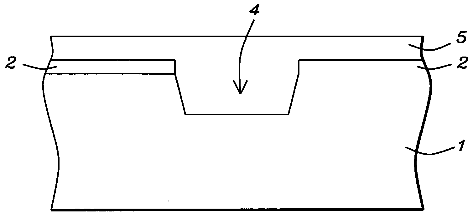
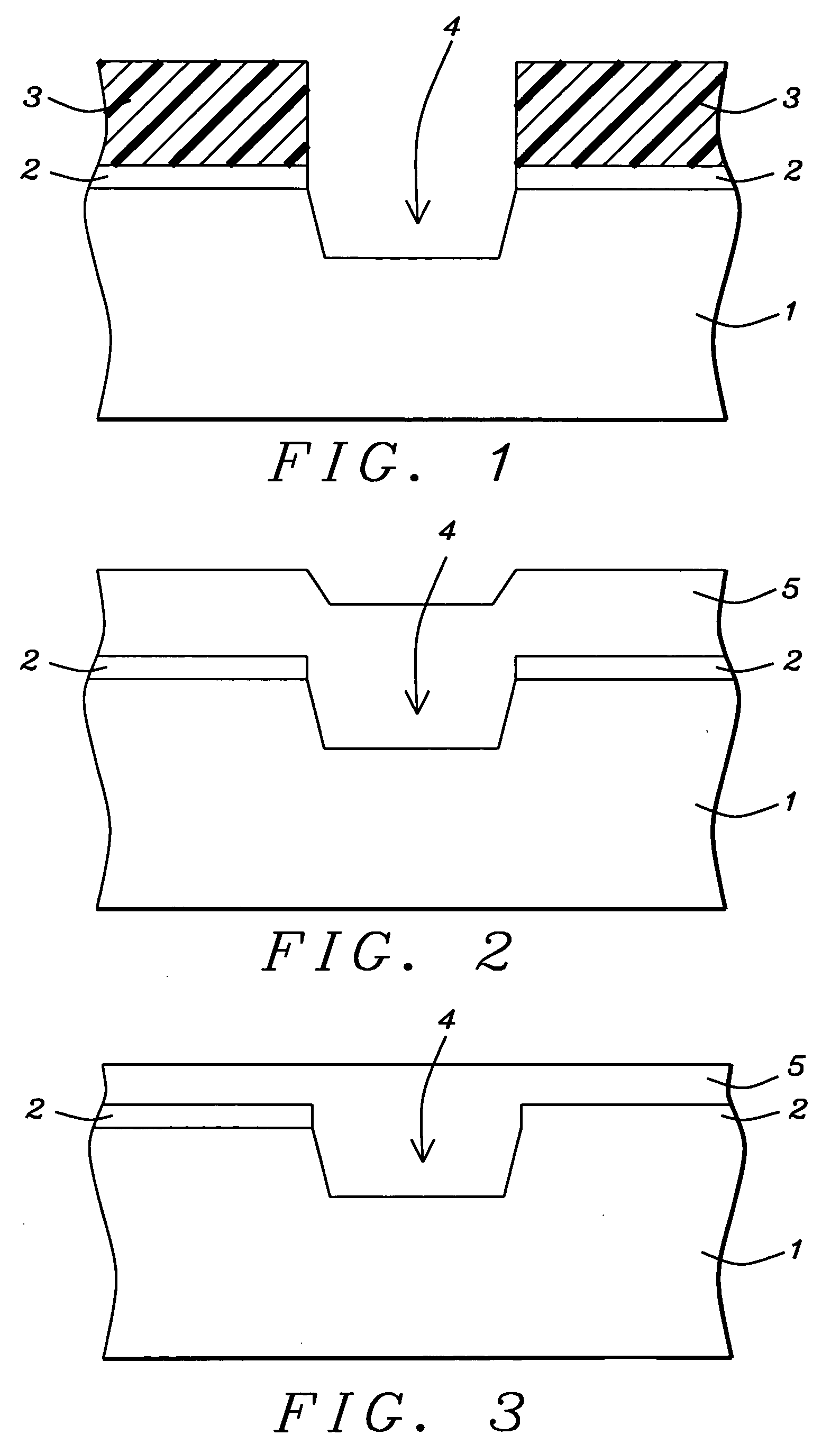
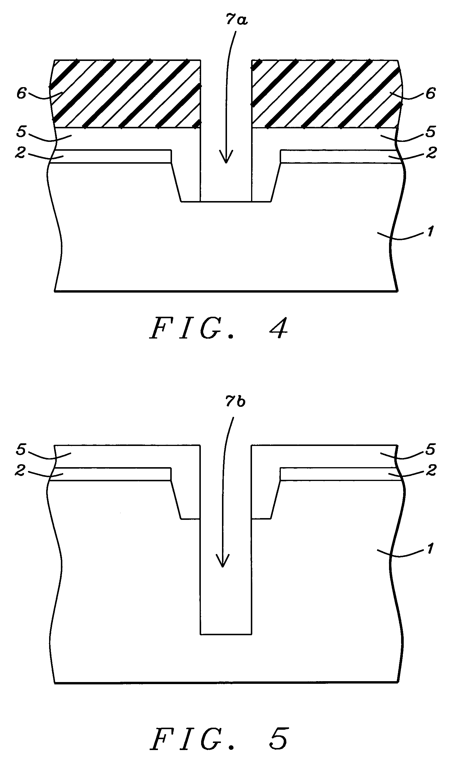
[0013] The method used to from a shallow trench-deep trench isolation region, featuring a combination of polishing, insulator filling, and patterning procedures employed to obtain a smooth top surface topography for the isolation region, will now be described in detail. Semiconductor substrate 1, comprised of P type single crystalline silicon, featuring a crystallographic orientation, is used and schematically shown in FIG. 1. Silicon nitride layer 2, is deposited at a thickness between about 1100 to 2000 Angstroms, via low pressure chemical vapor deposition (LPCVD), or via plasma enhanced chemical vapor deposition (PECVD), procedures. Photoresist shape 3, is then used as an etch mask allowing a dry etch procedure to define shallow trench opening 4, in silicon nitride layer 3, and to a depth between about 3000 to 5000 Angstroms in a top portion of semiconductor substrate 1. The dry etching procedure is accomplished using Cl2 as an etchant for both silicon nitride and silicon, with ...
PUM
 Abstract
Description
Claims
Application Information