Buried guard ring and radiation hardened isolation structures and fabrication methods

a technology of radiation hardening isolation structure and guard ring, which is applied in the direction of semiconductor devices, semiconductor/solid-state device details, electrical apparatus, etc., can solve the problems of complete destructive failure of integrated circuits (ics), sporadic device behavior, and electrical degradation, and achieves reduced or eliminated detrimental effects, low cost, and relative simplicity

Active Publication Date: 2005-08-18
SILICON SPACE TECH
View PDF45 Cites 115 Cited by
  • Summary
  • Abstract
  • Description
  • Claims
  • Application Information

AI Technical Summary

Benefits of technology

[0011] It has been discovered that semiconductor devices can be fabricated using conventional designs and process but including specialized structures to reduce or eliminate detrimental effects caused by various forms of radiation. Such semiconductor devices can include the one or more parasitic isolation ...

Problems solved by technology

Exposure to radiation causes electrical degradation of both transistors and circuit-isolation elements, which can lead to sporadic device behavior and/or complete destructive failure of integrated circuits (ICs).
The more limited low-volume demand for radiation-hardened ICs cannot justify the expense of dedicated leading-edge manufacturing facilities, despite the very attractive margins in the military and aerospace electronics market.
These financial constraints have severely limited the ability of radiation-hardened IC suppliers to utilize leading-edge IC manufacturing technology.
Consequently, the number of companies producing radiation-hardened IC components has been dramatically reduced, and their capabilities have fallen far behind those o...

Method used


Image

  • Buried guard ring and radiation hardened isolation structures and fabrication methods
  • Buried guard ring and radiation hardened isolation structures and fabrication methods
  • Buried guard ring and radiation hardened isolation structures and fabrication methods

Examples


Embodiment Construction

[0027] The following sets forth a detailed description of at least the best contemplated mode for carrying out the one or more devices and / or processes described herein. The description is intended to be illustrative and should not be taken to be limiting.

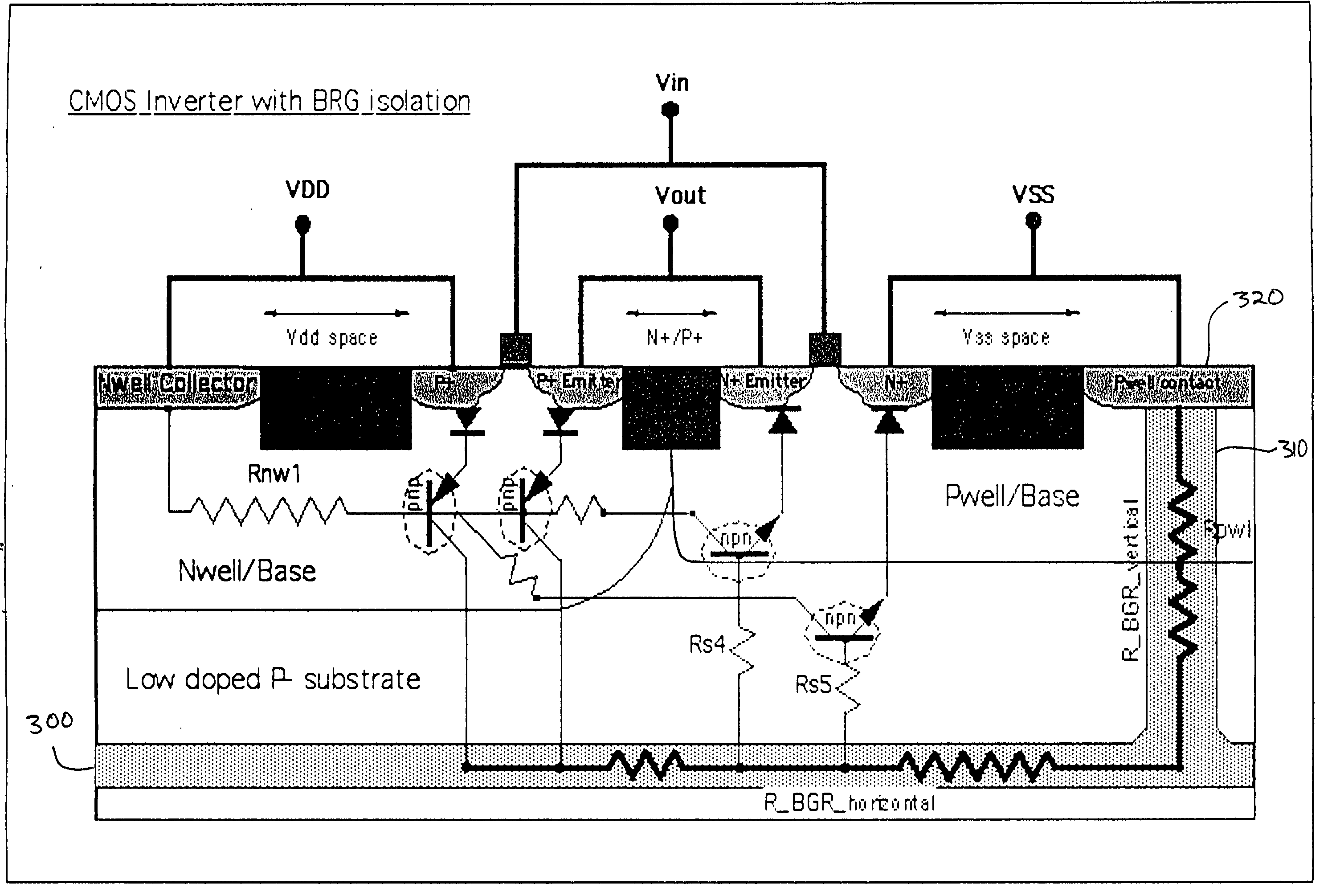
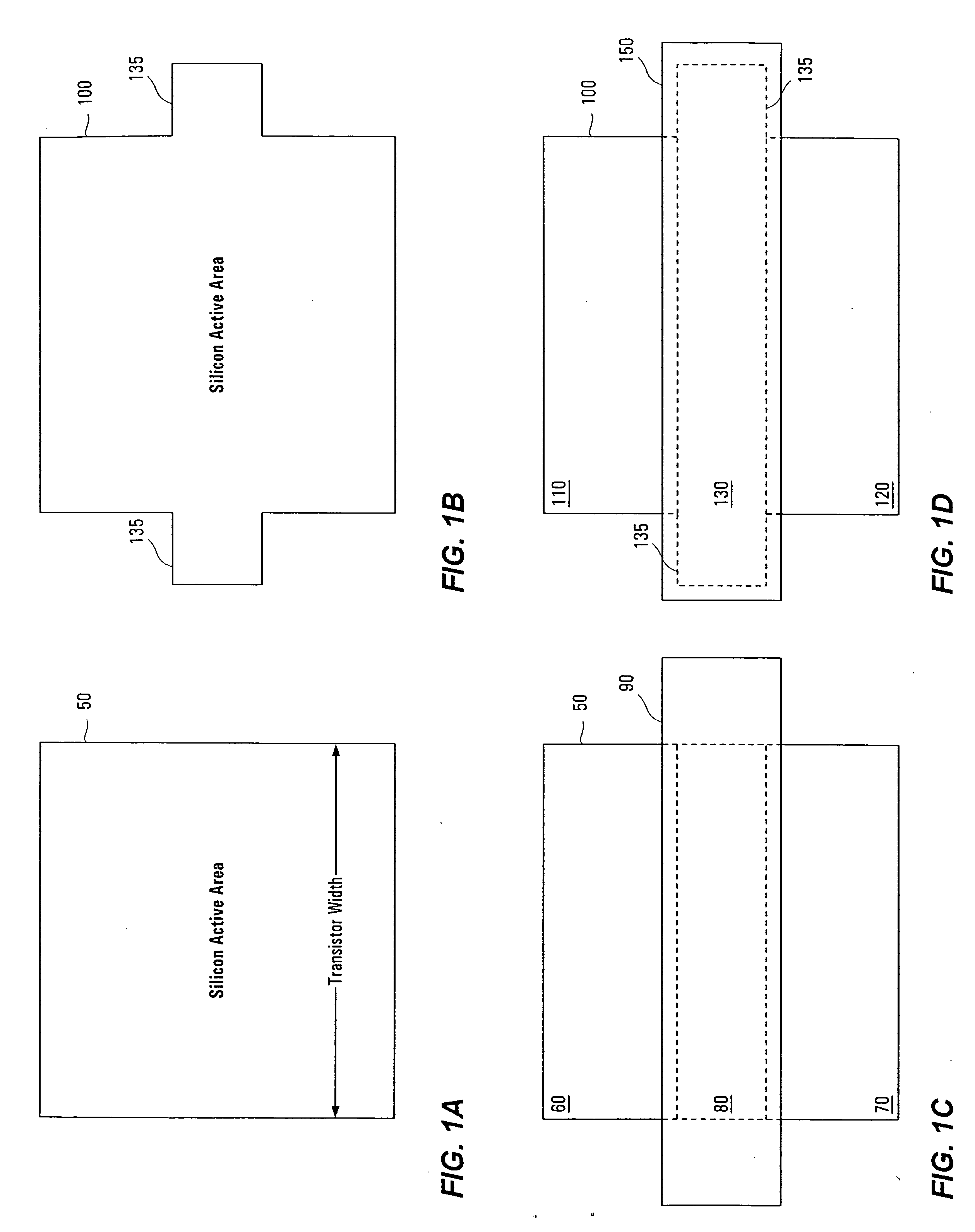
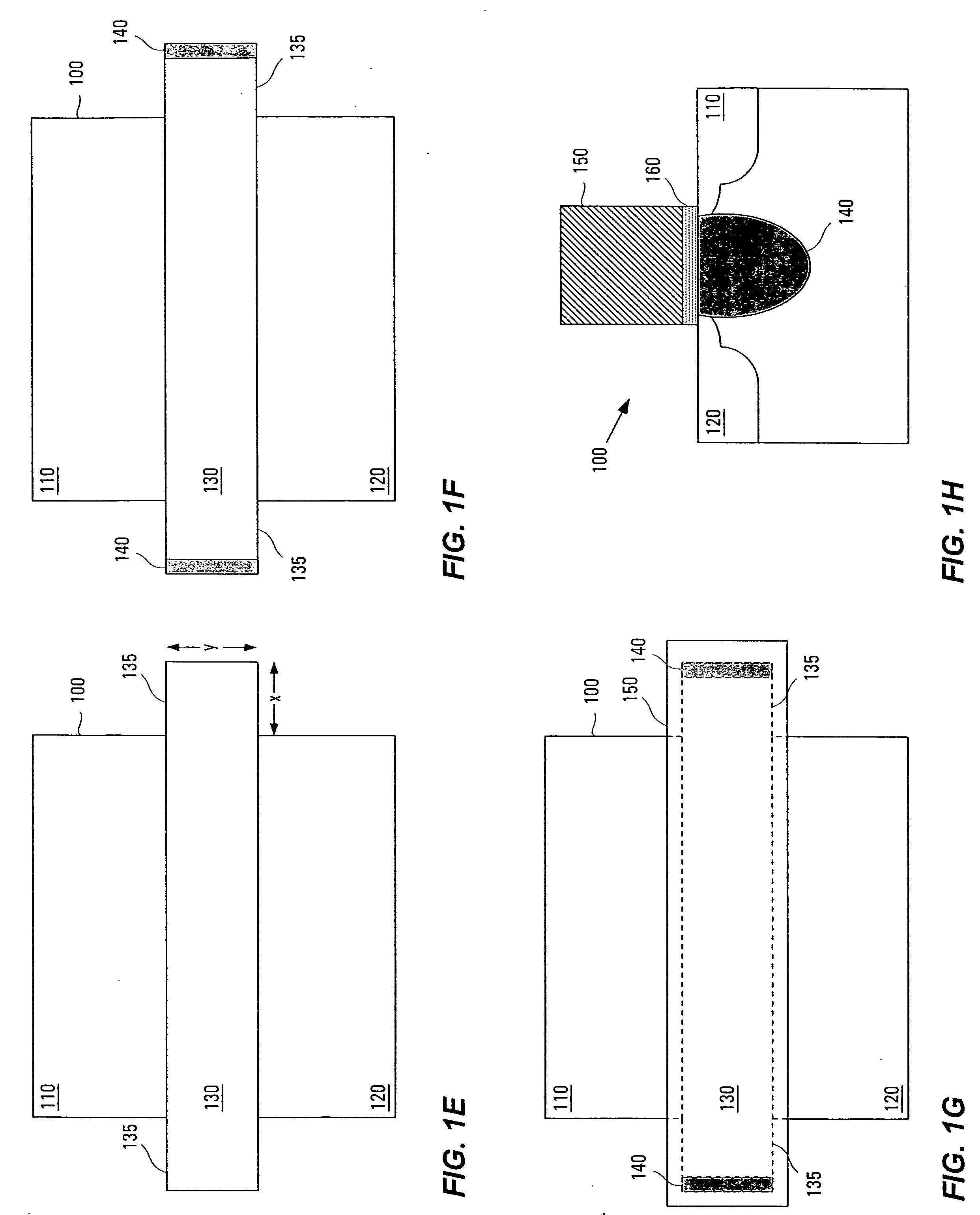
[0028] The devices and techniques described in the present application can deliver a complete radiation solution, or in some cases a specialized radiation solution, by directly addressing one or more of the primary degradation radiation effects of ICs: Total Ionizing Dose (TID), Single Event Latch-up (SEL), and Single-Event Upset (SEU). Moreover, the solutions to these degradation mechanisms are accomplished at the silicon process level with modifications to existing foundry baseline process. These unique approaches can be integrated into any CMOS process flow without affecting the performance of the underlying baseline technology. These approaches can further take advantage of a variety of different IC fabrication technologies, s...


PUM


Abstract

Semiconductor devices can be fabricated using conventional designs and process but including specialized structures to reduce or eliminate detrimental effects caused by various forms of radiation. Such semiconductor devices can include the one or more parasitic isolation devices and/or buried guard ring structures disclosed in the present application. The introduction of design and/or process steps to accommodate these novel structures is compatible with conventional CMOS fabrication processes, and can therefore be accomplished at relatively low cost and with relative simplicity.

Description

[0001] This application claims the benefit, under 35 U.S.C. § 119 (e), of U.S. Provisional Application No. 60 / 545,271, filed Feb. 17, 2004, entitled “Buried Guard Ring And Radiation Hardened Isolation Structures And Fabrication Methods,” and naming Wesley H. Morris as the inventor. The above-referenced application is hereby incorporated by reference herein in their entirety.BACKGROUND OF THE INVENTION [0002] 1. Field of the Invention [0003] The present invention relates to integrated circuits, and particularly to integrated circuits with partial and / or complete immunity to failure modes associated with radiation exposure. [0004] 2. Description of the Related Art [0005] The high radiation environments, including the upper atmosphere, near-earth orbit, outer space, and certain terrestrial environments (e.g., proximity to devices producing significant amounts of radiation) provide the most hostile environments for reliable operation of microelectronic solid-state devices. Exposure to r...

Claims


Application Information

Patent Timeline
IPC IPC(8): H01L21/336H01L21/74H01L21/761H01L23/06H01L27/092H01L29/76H01L29/94H01L31/062H01L31/113H01L31/119
CPCH01L21/761H01L27/0921H01L29/1083H01L29/1087H01L23/552H01L2924/0002H01L29/66477H01L2924/00
Inventor MORRIS, WESLEY H.
Owner SILICON SPACE TECH
Why Eureka
Try Eureka