Organic electro-luminescent display device and method of manufacturing the same

Active Publication Date: 2005-08-18
SAMSUNG DISPLAY CO LTD
View PDF16 Cites 109 Cited by
  • Summary
  • Abstract
  • Description
  • Claims
  • Application Information

AI Technical Summary

Benefits of technology

[0025] It is still an object of the present invention to provide an OELD device that prevents voltage drops of a power line (VDD) and a cathode using an auxiliary power line and a method of manufacturing the same.
[0026] It is further an object o

Problems solved by technology

Therefore, the transparent conductive film has poor film quality and has a high specific resistance.
When the specific resistance of a cathode is high, a non-uniform cathode voltage can be applied to the pixels and can generate a voltage difference between a location close to the power supply point and a location remote from the power supply point due to a voltage drop.
The voltage difference can cause non-uniform brightness and image characteristics, and increases power consumption.
The voltage drop is also a reason that makes it difficult to manufacture a large size AM OELD device.
However, the OELD device can solve the problem of non-uniform brightness caused by the voltage

Method used


Image

  • Organic electro-luminescent display device and method of manufacturing the same
  • Organic electro-luminescent display device and method of manufacturing the same
  • Organic electro-luminescent display device and method of manufacturing the same

Examples


first embodiment

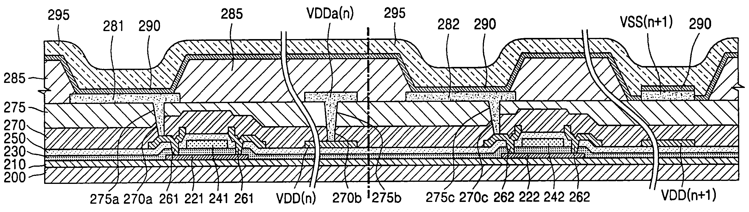
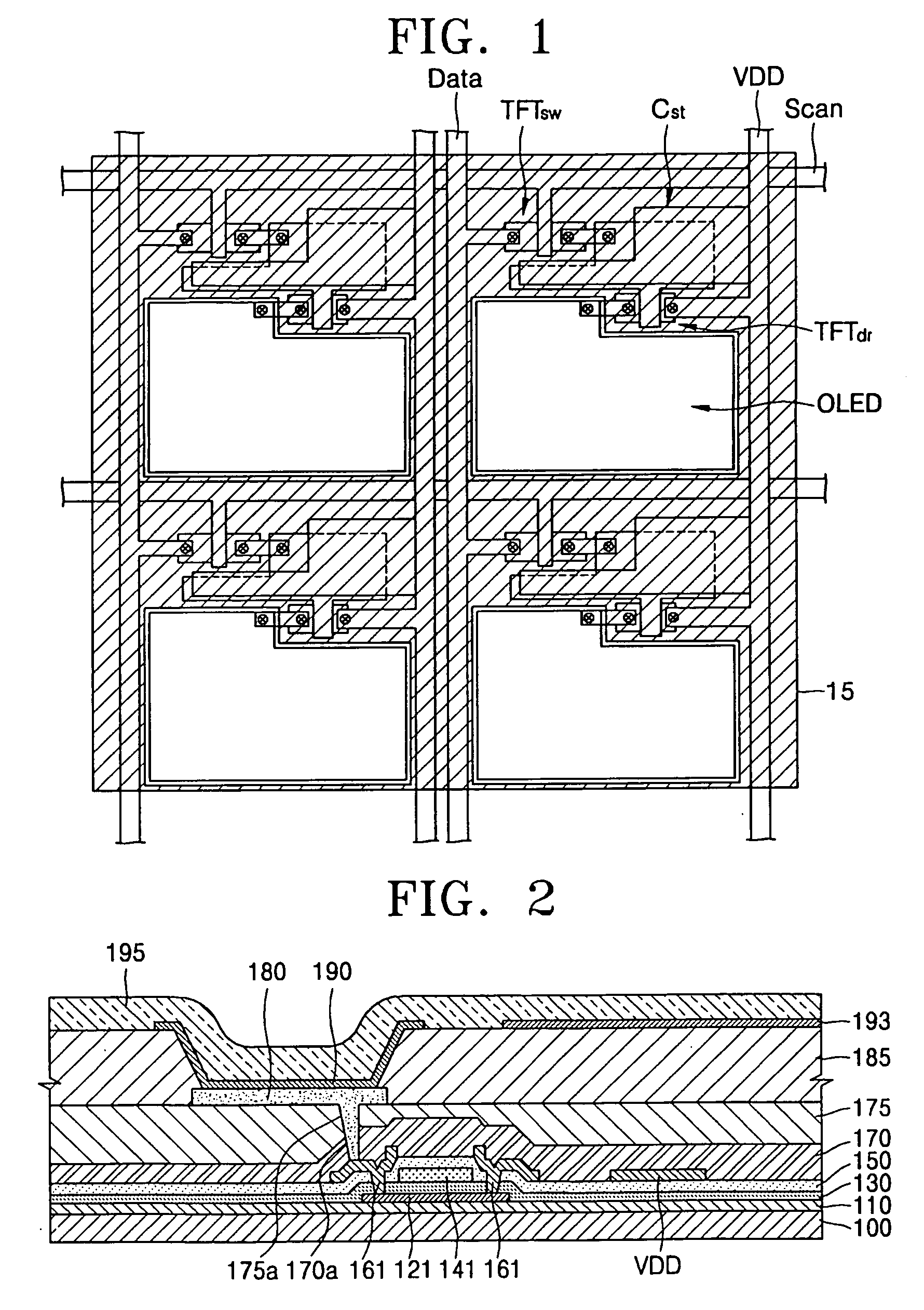
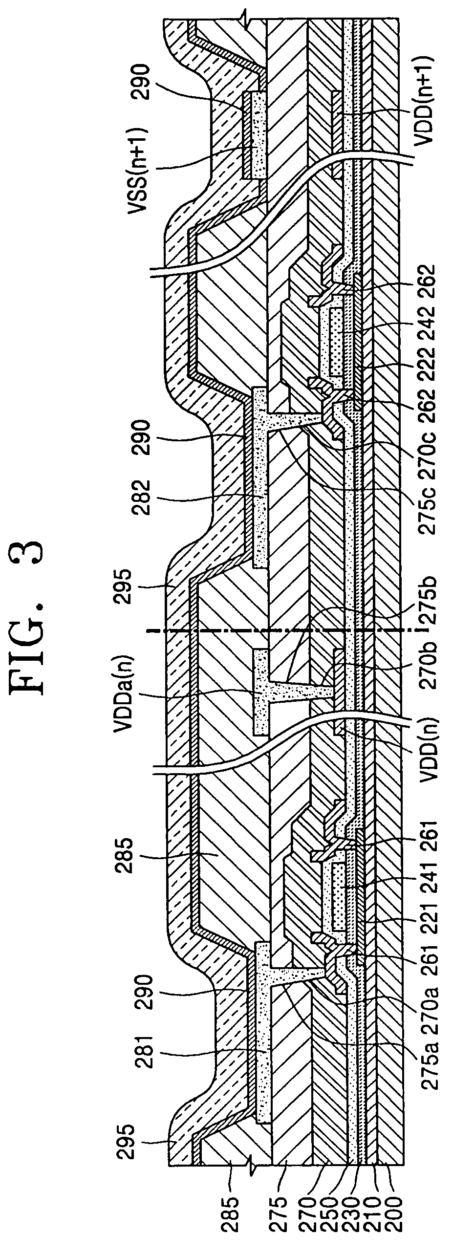
[0053]FIG. 3 is a cross-sectional view showing structures of pixels arranged in an nth column and (n+1)th column of an OELD device according to the present invention.

[0054] Referring to FIG. 3, the OELD device according to a first embodiment of the present invention includes a buffer layer 210 formed on a substrate 200, a thin film transistor (TFT) (hereinafter a first TFT) of a pixel arranged in an nth column and a TFT (hereinafter a second TFT) of a pixel arranged in an (n+1)th column. The first and second TFTs are disposed on the buffer layer 210. The substrate can be an insulating substrate that includes glass or plastic or a metal substrate.

[0055] The first TFT includes a semiconductor active layer 221, a gate electrode 241, source and drain electrodes 261, and the second TFT includes a semiconductor active layer 222, a gate electrode 242, and source and drain electrodes 262.

[0056] A gate insulating layer 230 is formed between the semiconductor active layers 221 and 222 and t...

second embodiment

[0072]FIG. 8 is a cross-sectional view showing structures of pixels disposed in an nth column and an (n+1)th column of an OELD device according to the present invention.

[0073] The AM OELD device depicted in FIG. 8 has a similar structure with the AM OELD device of the first embodiment. The difference between them is that the organic film 290 in the first embodiment is formed on the entire surface of the substrate, and the upper electrode 295 is electrically connected to the side surfaces of the second auxiliary power line (VSS(n+1)), but an upper electrode 395 in the second embodiment is electrically connected to the side surfaces and the upper surface of the second auxiliary power line (VSS(n+1)) since an organic film 390 in the second embodiment is formed only on lower electrodes 381 and 382 not on the second auxiliary power line (VSS(n+1)).

[0074] At this time, the organic film 390 can be formed only on the opening of a pixel defining film 385 formed on an edge portion of the low...


PUM

PropertyMeasurementUnit
Reflectanceaaaaaaaaaa
Timeaaaaaaaaaa
Thicknessaaaaaaaaaa

Abstract

An organic electroluminescence device which includes a power line formed on the same layer as source and drain electrodes of a thin film transistor (TFT) and formed on a substrate on which the TFT is formed, a first insulating layer formed on the TFT, a lower electrode that electrically connected to one of the source and drain electrodes of the TFT and disposed on the first insulating layer, a first auxiliary power line and a second auxiliary power line formed on the same layer as the lower electrode in the second insulating layer, a second insulating layer formed on an edge portion of the lower electrode and not formed on the second auxiliary power line, wherein an opening that exposes a portion of the lower electrode is formed, an organic film formed on a substrate; and an upper electrode formed on the substrate.

Description

CLAIM OF PRIORITY [0001] This application claims the priority of Korean Patent Application No. 10-2004-0009842, filed on Feb. 14, 2004, in the Korean Intellectual Property Office, the disclosure of which is incorporated herein in its entirety by reference. BACKGROUND OF THE INVENTION [0002] 1. Field of the Invention [0003] The present invention relates to an organic electroluminescence display device and a method of manufacturing the same, and more particularly, to an organic electroluminescence display device that can be formed with a large size screen and can prevent non-uniform brightness of a panel using an auxiliary power line to prevent a voltage drop of a power line and an upper electrode and a method of manufacturing the same. [0004] 2. Description of the Related Art [0005] Since organic electroluminescence display (OELD) devices are emissive display devices that emit light by electrically exciting an organic fluorescent compound, can be driven at a low driving voltage, are ...

Claims


Application Information

Patent Timeline
IPC IPC(8): G09F9/30H05B33/10G09G3/32H01L27/32H01L51/50H05B33/26
CPCH01L51/5234H01L27/3276H10K59/1315H10K50/824H10K50/828B43K19/14B43K19/02B43K19/16C09J11/06C09J161/04
Inventor KWAK, WON-KYU
Owner SAMSUNG DISPLAY CO LTD
Why Eureka
Try Eureka