Non-volatile semiconductor memory device

Inactive Publication Date: 2005-08-18
PANASONIC CORP
View PDF11 Cites 21 Cited by
  • Summary
  • Abstract
  • Description
  • Claims
  • Application Information

AI Technical Summary

Benefits of technology

[0023] Therefore, an object of the present invention is to provide a non-volatile semiconductor memory device that has a

Problems solved by technology

Consequently, the potential of the main bit line MOi is not substantially increased.
This parasitic capacitance is a factor that may delay a data read operation.
More specifically, when the parasitic capacitance is large, the delay amount during a data read becomes large, and when the parasitic capacitance is small, the delay amount during a data read becomes small.
Therefore, unlike the memory cell, it is difficult to connect the reference cell to the main bit lines, which are connected to a plurality of memory cells a

Method used


Image

  • Non-volatile semiconductor memory device
  • Non-volatile semiconductor memory device
  • Non-volatile semiconductor memory device

Examples


first embodiment

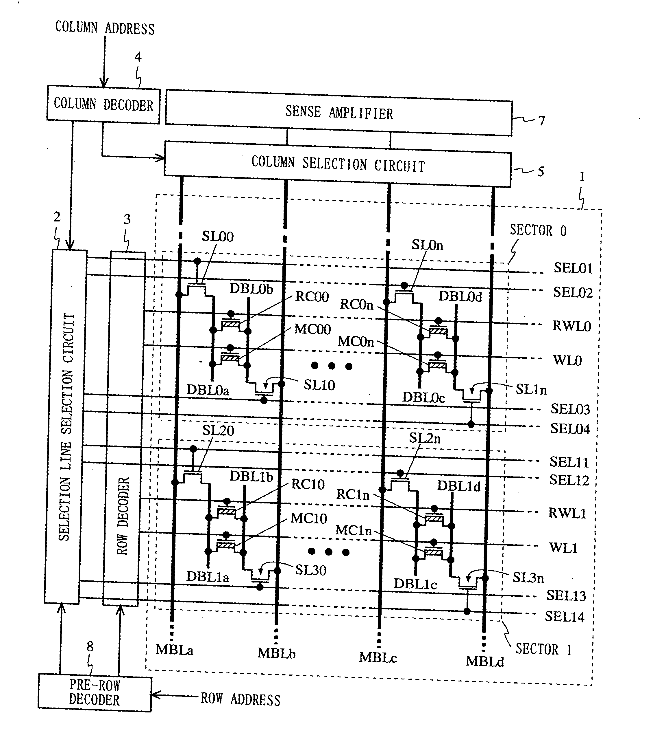
[0080] A non-volatile semiconductor memory device of a first embodiment of the present invention will be described with reference to the accompanying drawings. The specific configuration of the non-volatile semiconductor memory device of this embodiment will be described later. The non-volatile semiconductor memory device of this embodiment has an effect of eliminating the unbalance between the parasitic capacitance associated with the main bit line connected to a memory cell to be read (hereinafter, referred to as “narrow sense-main bit line”) and the parasitic capacitance associated with the main bit line connected to a reference cell (hereinafter, referred to as “complementary main bit line”) during a read operation. FIG. 1 is a diagram showing the configuration of the non-volatile semiconductor memory device of this embodiment. The non-volatile semiconductor memory device of this embodiment is characterized by the read operation, so that, in the following, the read operation wil...

second embodiment

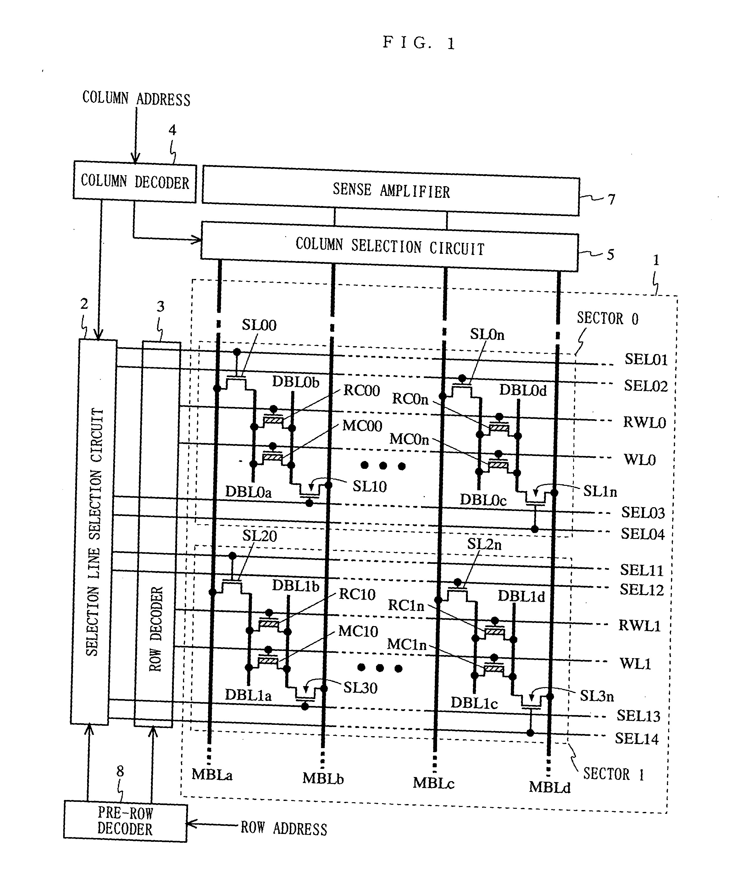
[0104] Hereinafter, a non-volatile semiconductor memory device of a second embodiment of the present invention will be described with reference to the accompanying drawings. A specific configuration of the non-volatile semiconductor memory device of this embodiment will be described later. The non-volatile semiconductor memory device of this embodiment is the same as the non-volatile semiconductor memory device of the first embodiment, except that the arrangement position of the reference cells is changed. FIG. 3 is a diagram showing the configuration of the non-volatile semiconductor memory device of this embodiment. Also in the non-volatile semiconductor memory device of this embodiment, the read operation will be described.

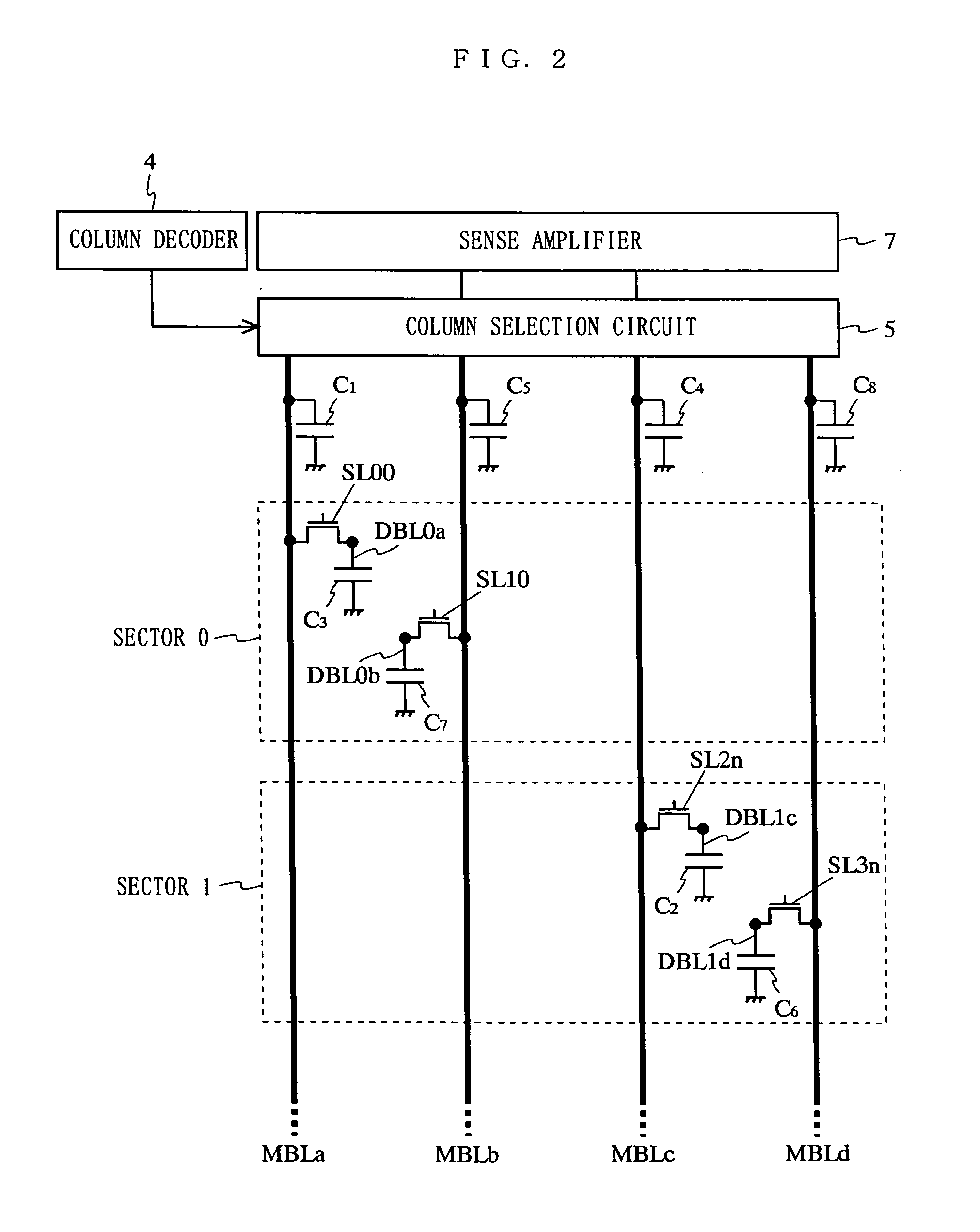
[0105] The non-volatile semiconductor memory device shown in FIG. 3 includes a memory cell area 9, a selection line selection circuit 2, a row decoder 3, a column decoder 4, a column selection circuit 5, a sense amplifier 7 and a pre-row decoder 8. In the memo...


PUM


Abstract

A plurality of memory cells are connected between two adjacent sub-bit lines. A row decoder 3 selects a word line connected to a memory cell to be read. A selection line selection circuit 2 and a column selection circuit 5 include first and second selection portions that perform selection operations simultaneously and independently. The first selection portion selects a first pair of main bit lines and selection lines in order to select the memory cell to be read. The second selection portion selects a second pair of main bit lines that is different from the first pair of main bit lines and selection lines for selecting a sector different from that for the memory cell to be read in order to select a line to be used for reading a reference voltage.

Description

BACKGROUND OF THE INVENTION [0001] 1. Field of the Invention [0002] The present invention relates to a non-volatile semiconductor memory device. More specifically, the present invention relates to a non-volatile semiconductor memory device having a matrix-shaped memory cell area including a plurality of memory cells arranged in a plurality of rows and a plurality of columns. [0003] 2. Description of the Background Art [0004] As one configuration of a non-volatile semiconductor memory device, VGA (virtual ground array) is known. The VGA configuration refers to a configuration in which adjacent memory cells share a diffusion layer. The area of the non-volatile semiconductor memory device can be reduced by adopting the VGA configuration. FIG. 17 shows a non-volatile semiconductor memory device having the VGA configuration. The non-volatile semiconductor memory device shown in FIG. 17 has the VGA configuration and has a hierarchical bit line structure including main bit lines and sub-bi...

Claims


Application Information

Patent Timeline
IPC IPC(8): G11C16/02G11C16/06G11C16/04
CPCG11C16/04
Inventor KOJIMA, MAKOTOMARUYAMA, TAKAFUMI
Owner PANASONIC CORP
Why Eureka
Try Eureka