

Method to simulate the influence of production-caused variations on electrical interconnect properties of semiconductor layouts
a technology of layout and variation, applied in the field of semiconductor technology, can solve the problems of increasing design complexity, affecting the accuracy and reliability of corresponding results, and the extraction process itself is of considerable complexity, so as to improve the accuracy and reliability of corresponding results, and the efficiency of extraction and simulation process.
- Summary
- Abstract
- Description
- Claims
- Application Information
AI Technical Summary
Benefits of technology
Problems solved by technology
Method used
Image

Examples
Embodiment Construction
[0046] The following detailed description of the invention relates directly to the drawings which are part of the specification.
[0047] The symbols used within the description are explained at the place of their introduction. The symbols are also summarized in a table at the end of the Brief Description of the Drawings.
[0048] The term “list” indicates a matrix of any size and dimension.
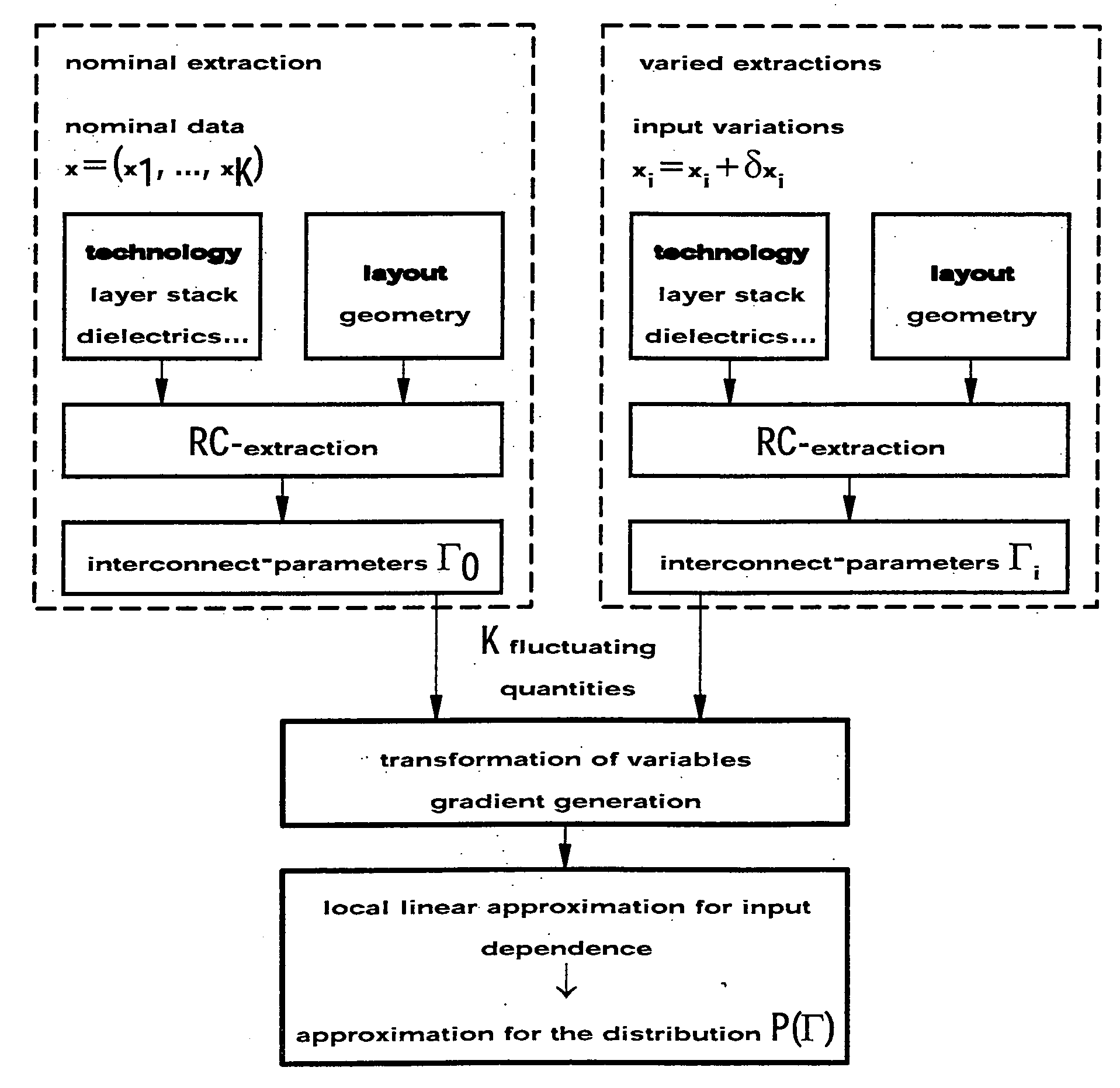
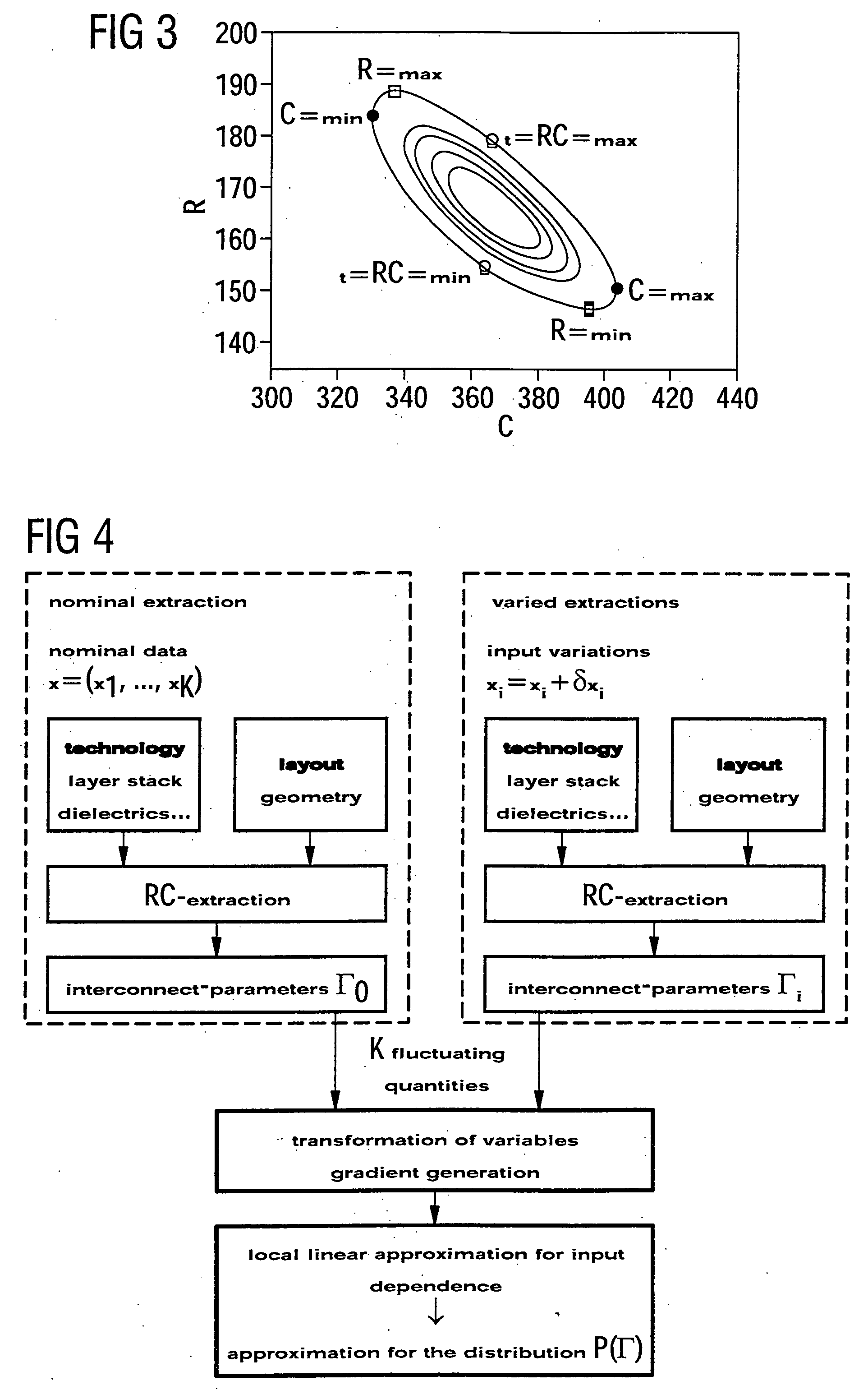
[0049] In a first embodiment, the invention relates to a method to simulate the influence of production-caused variations on semiconductor layouts.
[0050] The inventive method is not limited to the field of semiconductor technologies, but is also suitable in other production processes wherein fluctuating process parameters cause correlated variations of production related target quantities.
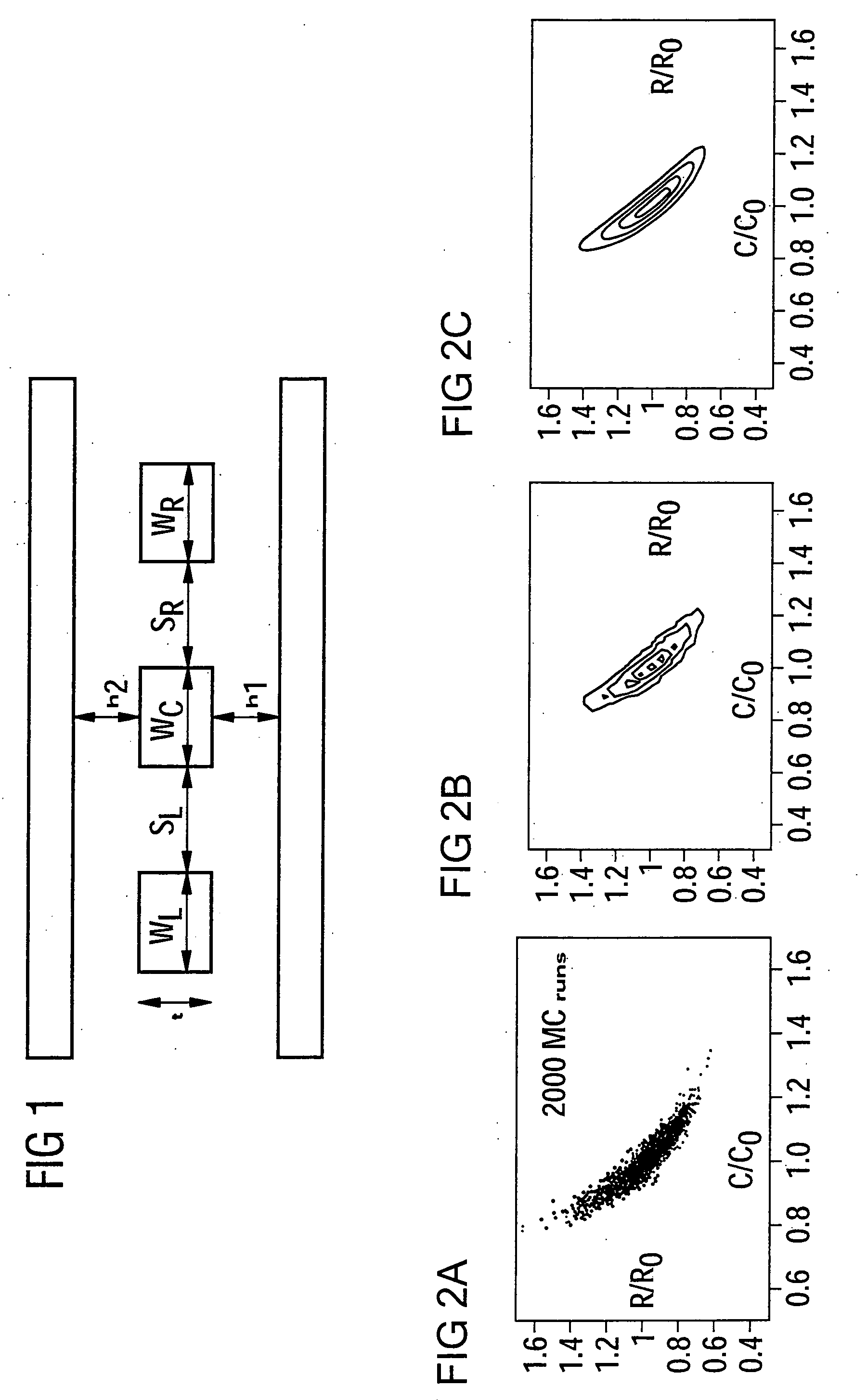
[0051] The basic input parameters are the material parameters and the given set of layout data. This data set is grouped to an input-vector x that includes the parameters x1, . . . , xK denoting the given data, e...
PUM
 Abstract
Description
Claims
Application Information