Method and apparatus for automating the design of programmable logic devices

a programmable logic and design method technology, applied in the direction of instruments, specific program execution arrangements, program control, etc., can solve the problems of increasing complexity, increasing size and complexity of fpgas, and relatively small fpgas, and achieve cost-effective effects

Inactive Publication Date: 2005-08-18
NORTEL NETWORKS LTD
View PDF5 Cites 41 Cited by
  • Summary
  • Abstract
  • Description
  • Claims
  • Application Information

AI Technical Summary

Benefits of technology

[0015] The present invention overcomes these and other drawbacks by providing a method and apparatus for automating the design of programmable logic devices. According to one embodiment of the invention, the automated process enables much of the design of programmable logic devices, such as Field Programmable Gate Arrays (FPGAs), to be automated without requiring extensive manual intervention during the iterative process of implementing the design on the FPGA. Accordingly, FPGA design may be accomplished much more quickly and in a more cost-effective manner.

Problems solved by technology

Traditionally, however, FPGAs have been relatively small and able to perform limited functionality.
As FPGAs have increased in size and complexity, they have become able to perform increasingly complex functions; they are starting to replace traditional ASICs and other circuit specific hardware.
As FPGAs have increased in size and capability, the ease to program them and the design process associated with optimizing a design on an FPGA has increased in complexity and design effort.
Unfortunately, this process requires considerable time and effort and contributes to the cost and time lag associated with implementing FPGA designs.

Method used


Image

  • Method and apparatus for automating the design of programmable logic devices
  • Method and apparatus for automating the design of programmable logic devices
  • Method and apparatus for automating the design of programmable logic devices

Examples


Embodiment Construction

[0023] The following detailed description sets forth numerous specific details to provide a thorough understanding of the invention. However, those skilled in the art will appreciate that the invention may be practiced without these specific details. In other instances, well-known methods, procedures, components, protocols, algorithms, and circuits have not been described in detail so as not to obscure the invention.

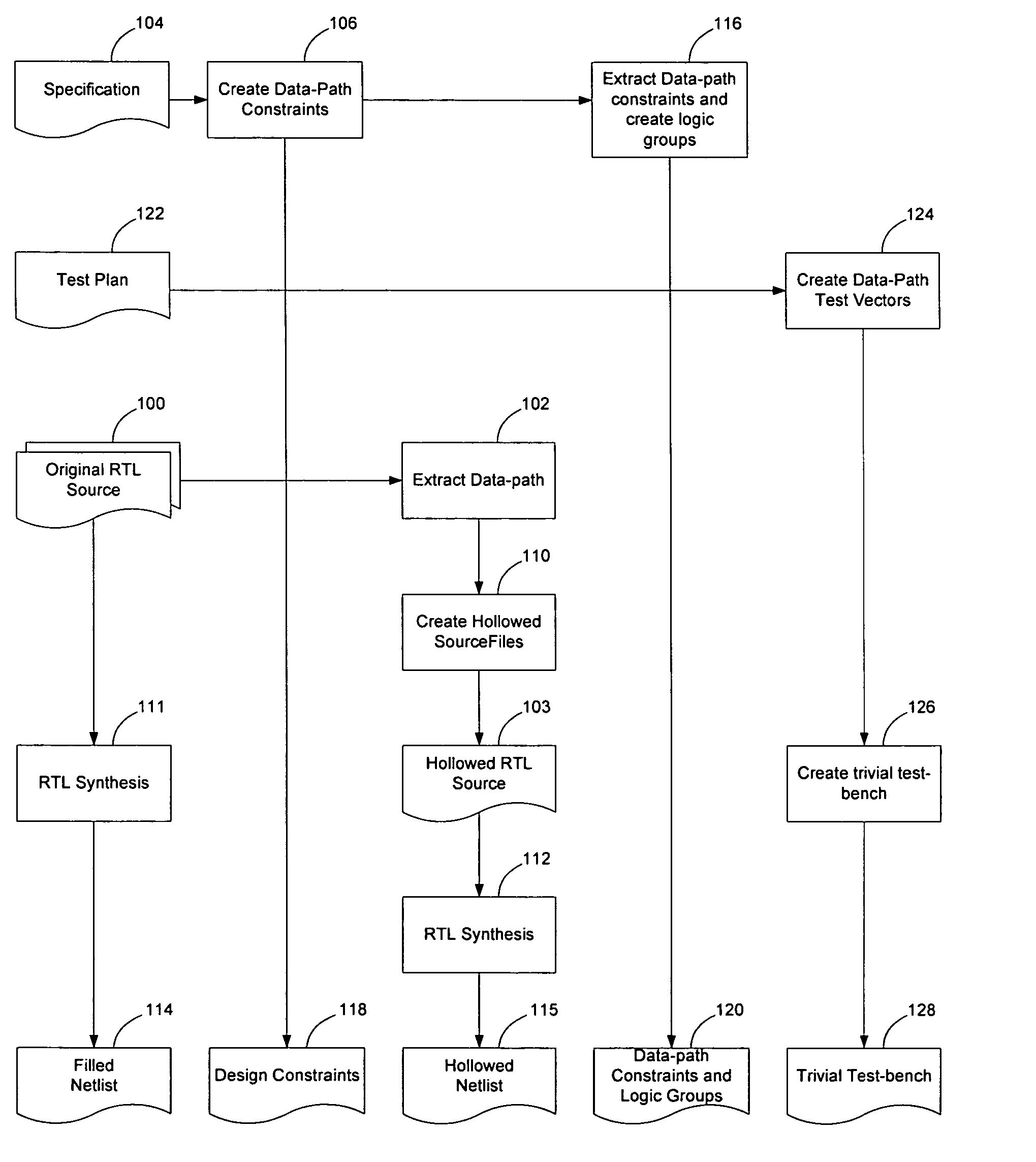
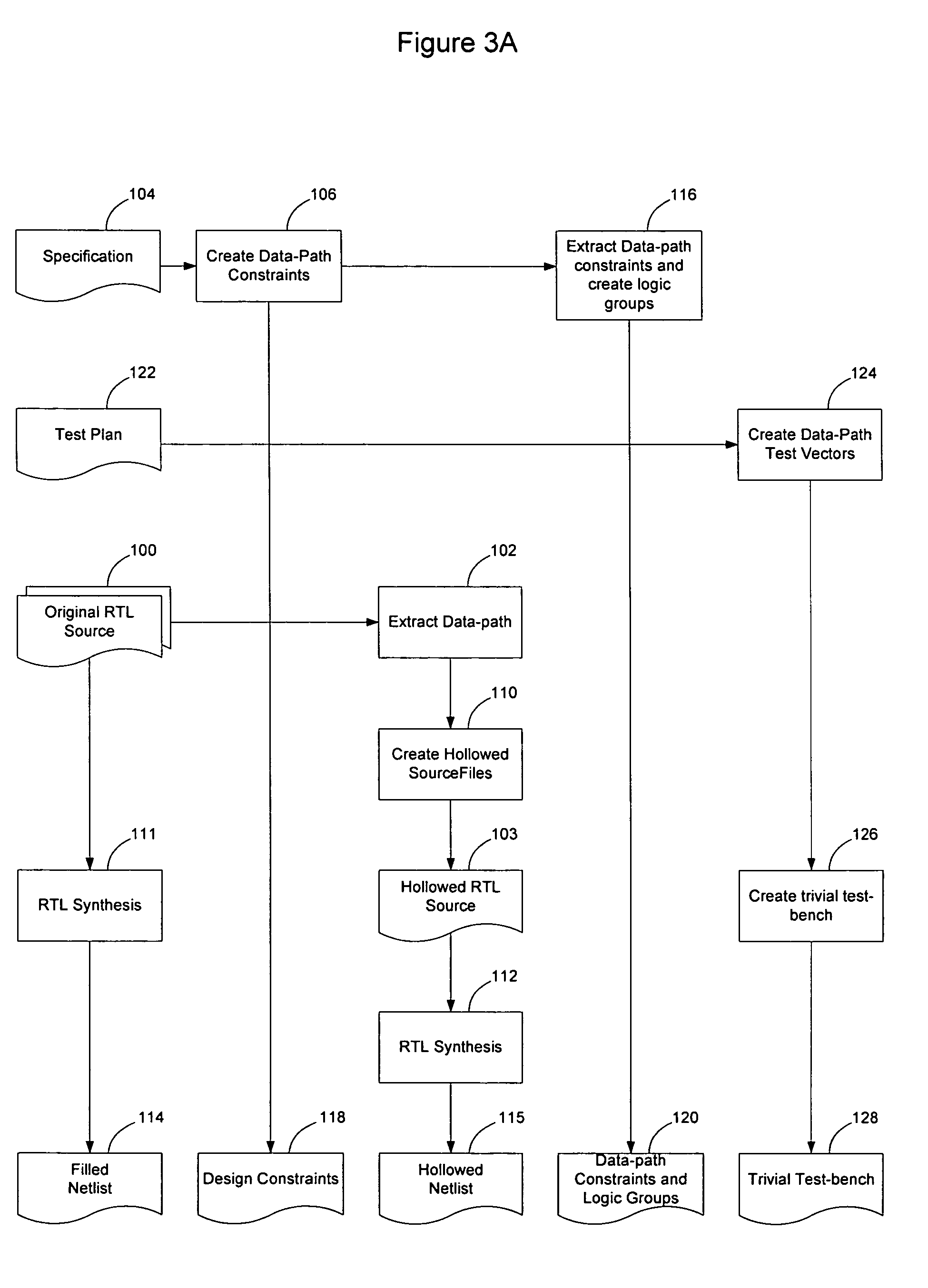
[0024] As described in greater detail below, an automated process for designing programmable logic devices, such as Field Programmable Gate Arrays (FPGAs), enables much of the design to be automated without requiring extensive manual intervention during the iterative process of implementing the design on the FPGA. Accordingly, FPGA design may be accomplished much more quickly and in a more cost-effective manner.

[0025] According to an embodiment of the invention, once a netlist has been generated in a standard fashion from a logic design, the implementation of that netl...


PUM


Abstract

The design of programmable logic devices, such as FPGAs, may be automated to allow scripts, setup files, and other tool files to be created directly from hollowed and filled netlist, and data-path and design constraint files without extensive human intervention. This allows an FPGA design to be created directly from a logic file to accelerate the FPGA design process. Once hollowed and filled netlists, and data-path and design constraint files have been generated from a design in a standard fashion, the implementation of that design onto an FPGA in an optimized fashion is automated by providing a computer program that is capable of implementing the design, testing the design, evaluating the test results, and altering the design to arrive at a more optimal design. The process may include several steps, such as initial placement of logic groups, sizing of logic groups and FPGA selection, timing analysis, and filled netlist complete design review. The steps may be iterative.

Description

BACKGROUND OF THE INVENTION [0001] 1. Field of the Invention [0002] The present invention relates to very large-scale integration (VLSI) circuit design and, more particularly, to a method and apparatus for automating the design of programmable logic devices. [0003] 2. Description of the Related Art [0004] Programmable Logic Devices are general purpose chips that may be configured for a wide variety of applications. Design implementation into a PLD device is done by programming the interconnection of its basic elements to perform the logic functions that embody the design. [0005] There are also many types of basic elements that may be included in a PLD. Several basic elements may be configured to enable conventional logic gates, such as AND gates or OR gates; while other PLD basic elements may be configured as memory elements, such as FIFOs or registers. Other configurations may exist as well and the invention is not limited to a particular type of PLD configuration. [0006] Field Pro...

Claims


Application Information

Patent Timeline
Patent Type & Authority Applications(United States)
IPC IPC(8): G06F17/50
CPCG06F17/5072G06F17/5054G06F30/34G06F30/392G06F2119/12G06F30/347
Inventor HERRERA, ALFREDO
Owner NORTEL NETWORKS LTD
Why Eureka
Try Eureka