
Flat panel display

a flat panel display and display panel technology, applied in the field of flat panel displays, can solve the problems of limiting the protection layer provided by the protection layer to the organic el device, the internal device is not protected sufficiently, and the organic light emitting layer is very susceptible to moisture, so as to reduce the size of the panel (substrat) and improve the sealing function

Active Publication Date: 2005-08-25
SAMSUNG DISPLAY CO LTD
View PDF6 Cites 162 Cited by
  • Summary
  • Abstract
  • Description
  • Claims
  • Application Information

AI Technical Summary

Benefits of technology

[0017] The present invention provides a display, and more particularly, an organic electroluminescent flat panel display, in which a panel (substrate) size is reduced and a sealing function is simultaneously improved.

Problems solved by technology

However, in the organic EL display, organic layers including the organic light emitting layer are very vulnerable to moisture.
The above problem generally occurs in conventional AM type organic EL displays, including the organic EL display of Japanese Laid-Open Patent No. 2000-173779.
However, in the AM display described above, the protection layer is just a thin film, so internal devices are not protected sufficiently.
In addition, there is a limit to the protection provided by the protection layer to the organic EL device, which should be protected completely from moisture.
Moreover, the display having the thin protection layer cannot be a front-emission display or a dual-emission display, which form images in a direction of the sealing member.
Thus, the apparatus has a complex structure and a high line resistance.

Method used


Image

  • Flat panel display
  • Flat panel display
  • Flat panel display

Examples


Embodiment Construction

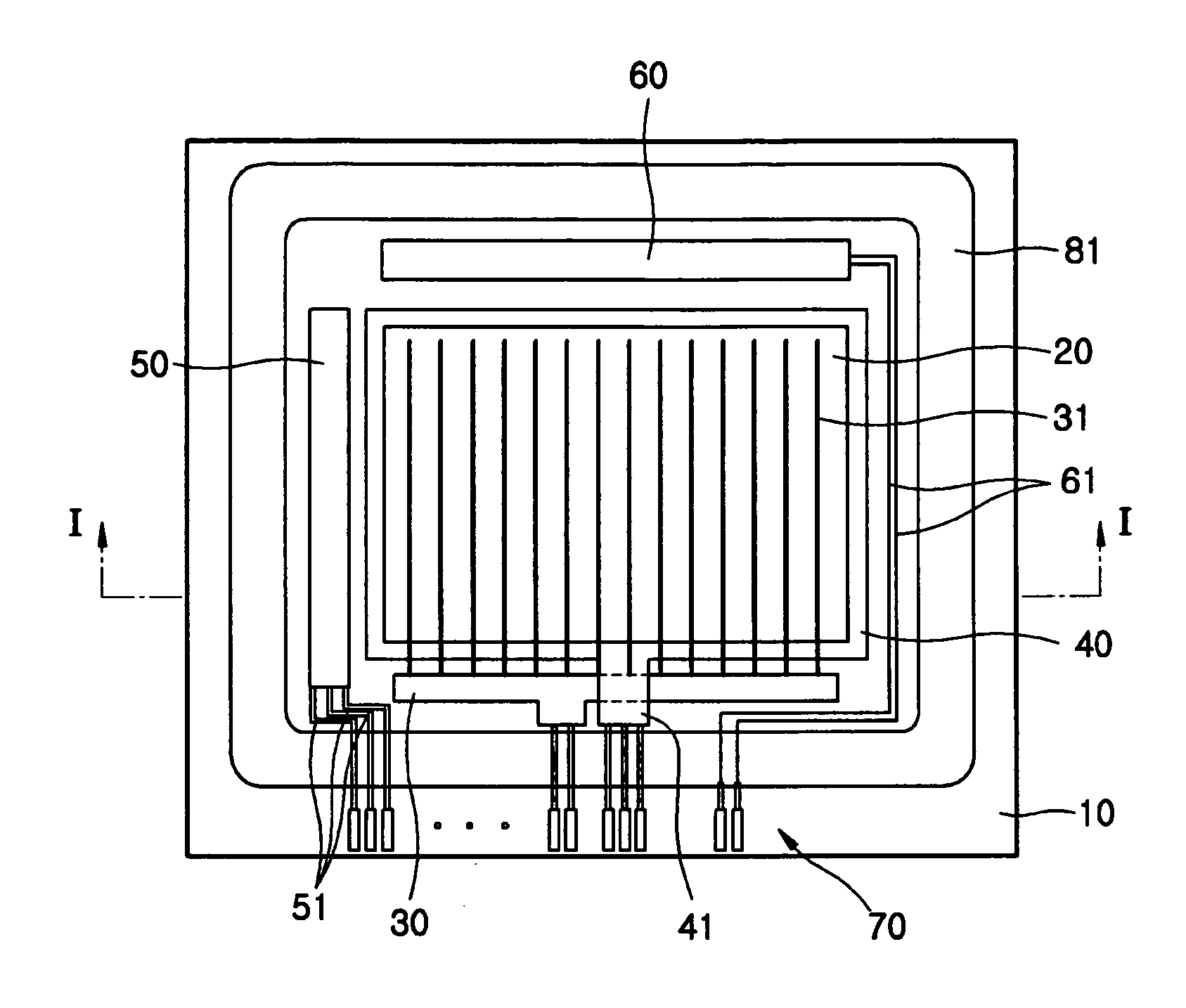
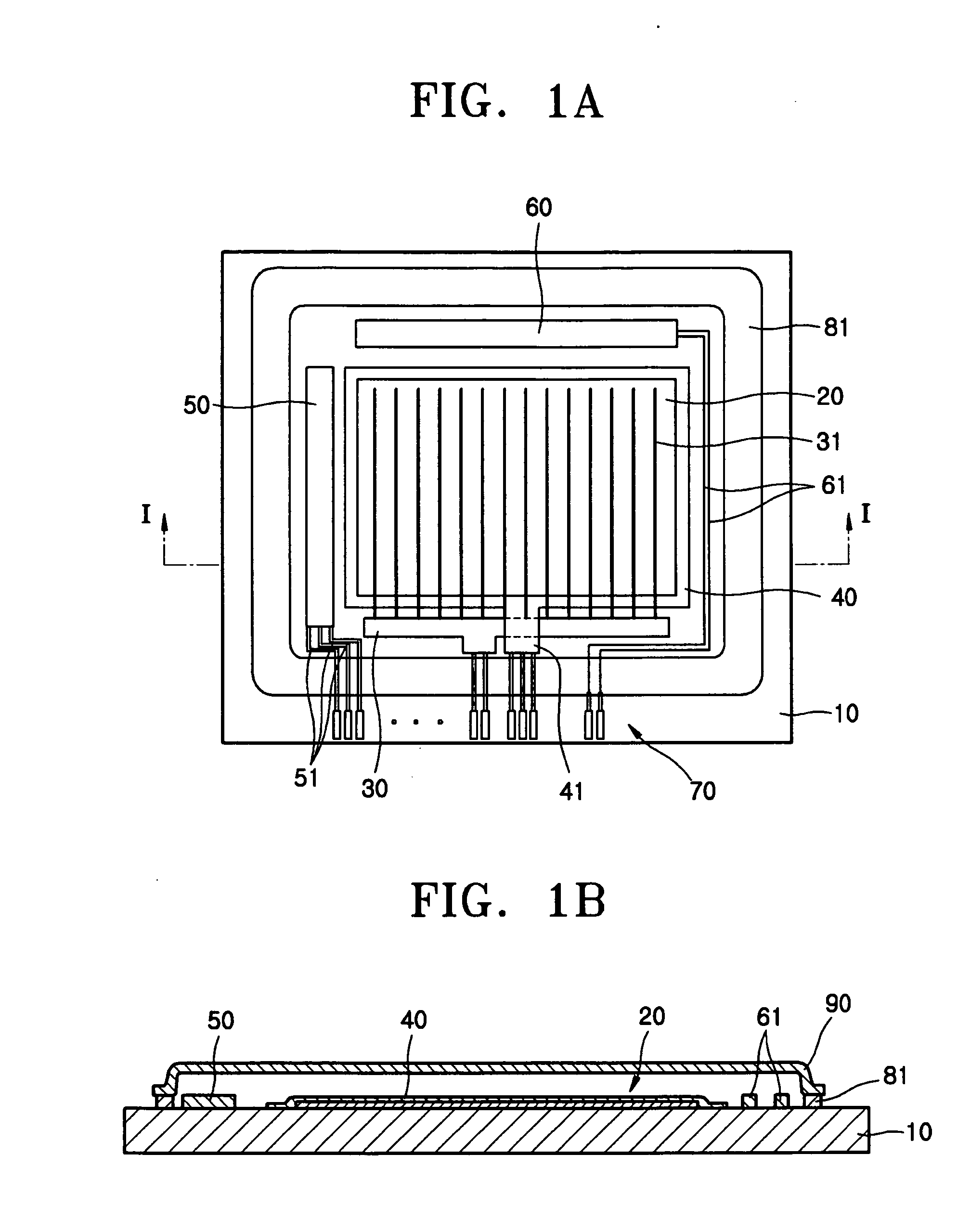
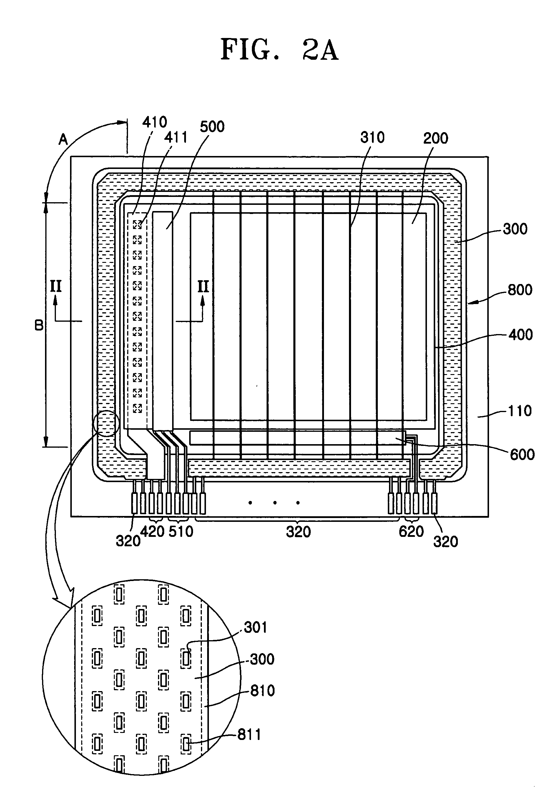
[0066]FIG. 2A is a view of a flat panel display, and more specifically, an organic electroluminescent (EL) display, according to an embodiment of the present invention. However, the present invention is not limited to the organic EL display of FIG. 2A.

[0067] The organic EL display of FIG. 2A includes a display area 200, on which a light emitting device, such as an organic EL device, is arranged on a substrate 110, a sealing portion 800 applied to an outer edge of the display area 200 to seal the substrate 110 and a sealing substrate (900 in FIG. 2B), and a terminal area, on which various terminals are arranged. The sealing portion 800 includes an edge portion (referred to as B in FIG. 2A) having four sides, and four corner portions (referred to as A in FIG. 2A).

[0068] Referring to FIG. 2B, the structure of the organic EL device in the display area 200 will now be described. A buffer layer 120 is formed on a substrate 110, for example, a glass substrate using SiO2. A semiconductor ...


PUM


Abstract

A display includes: a display area adapted to form an image with display devices arranged on a substrate; a sealing portion adapted to seal at least the display area with a sealant arranged along an outer edge portion of the display area; and a driving power supply line adapted to supply a driving voltage to the display area. The driving power supply line includes at least one conductive layer, at least a portion thereof being arranged between the sealing portion and the substrate. Each conductive layer includes at least one penetration hole.

Description

CLAIM OF PRIORITY [0001] This application makes reference to, incorporates the same herein, and claims all benefits accruing under 35 U.S.C. §119 from an application for FLAT PANEL DISPLAY DEVICE earlier filed in the Korean Intellectual Property Office on Feb. 14, 2004 and Feb. 18, 2004 and there duly assigned Ser. No(s). 2004-9843 and 2004-10670, respectively.BACKGROUND OF THE INVENTION [0002] 1. Field of the Invention [0003] The present invention relates to a display, and more particularly, to a flat panel display having a wide display area at least partially impervious to degradation caused by moisture. [0004] 2. Description of the Related Art [0005] Flat panel displays, such as liquid crystal displays, organic electroluminescent displays, and inorganic electroluminescent displays can be classified as either Passive Matrix (PM) displays and Active Matrix (AM) displays according to the driving method thereof. In the PM display, positive electrodes and negative electrodes are arran...

Claims


Application Information

Patent Timeline
IPC IPC(8): G09F9/30G09G3/12H01L27/32H01L51/52H05B33/04H05B33/12H05B44/00H05K7/00
CPCG09G2300/0426H01L51/5237H01L27/3276H01L27/124H10K59/131H10K59/8722H10K50/8426
Inventor KWAK, WON-KYU
Owner SAMSUNG DISPLAY CO LTD
Features
  • Generate Ideas
  • Intellectual Property
  • Life Sciences
  • Materials
  • Tech Scout
  • Unparalleled Data Quality
  • Higher Quality Content
  • 60% Fewer Hallucinations
Learn More