System and method of controlling power consumption in an electronic system

a technology of electronic system and power consumption, applied in the field of control of power consumption in electronic system, can solve the problems of power consumption becoming a major obstacle for circuit and system designers, power management problems for system designers, and power management problems taking form

Active Publication Date: 2005-08-25
IBM CORP
View PDF24 Cites 134 Cited by
  • Summary
  • Abstract
  • Description
  • Claims
  • Application Information

AI Technical Summary

Benefits of technology

[0023] Further and still other objects of the present invention will become more readily apparent when the following detailed description is taken in conjunction with the accompanying drawing figures.

Problems solved by technology

Power consumption increasingly has become a major obstacle to circuit and system designers.
This substantial increase in power density causes power management problems for system designers.
Power management problems take form in both heat dissipation and battery life issues.
Greater power dissipated by ICs with ever decreasing area causes significant temperature control issues at the system level.
The problem has become so pervasive that conventional forced air cooling systems are no longer able to dissipate the power generated by modern ICs.
Increased power consumption also creates battery life issues in portable systems and can significantly impact the usefulness of portable devices.
Further complicating increases in IC power consumption is manufacturing test.
Cost considerations limit the amount of test time that can be dedicated to each IC.
Manufacturing test cost concerns often limit the amount of characterization testing that can be done on any one IC (testing the part across a range of temperature, voltage and frequency to ensure robust operation).
Although a few of these processors may operate marginally at those conditions (and some will fail), most that function at those minimum requirements will operate well beyond those limits.
However, because of time constraints, this maximum operating speed is not determined.
Beyond these conditions, the IC no longer functions properly.
By limiting manufacturing testing to pass / fail testing at worst-case system requirements, end system power consumption is adversely affected in two ways: (1) most ICs that function at the minimum system speed at test will function well beyond it in the end system and (2) most ICs do not operate at the maximum system temperatures at which they are typically tested; and thus, their operating voltage may be lowered.
Additionally, variations in the tester environment may also add to measurement inaccuracies.
This problem is exasperated in portable devices because battery life is unnecessarily degraded when an IC is operated at worst-case system conditions although the system rarely (or never) actually operates at such worst-case conditions and the IC is capable of functioning properly below the worst-case conditions.
This patent does not teach or suggest a means for adjusting operating voltage based upon tester-to-system variations, worst-case testing techniques, or process variations.
Furthermore, this patent does not teach or suggest the use of a built-in-self-test engine for determining the minimum operating voltage of an integrated circuit throughout its useful life.
For example, if the processor is “docked” into a system that has cooling capabilities, the processor can be run at lower operating conditions, thereby lowering power.
This patent does not teach or suggest a means for adjusting operating voltage based upon tester-to-system variations, worst-case testing techniques, or process variations.
Furthermore, this patent does not teach or suggest the use of a built-in-self-test engine for determining the minimum operating voltage of an integrated circuit throughout its useful life.
This patent does not teach or suggest a means for adjusting operating voltage based upon tester-to-system variations, worst-case testing techniques, or process variations.
Furthermore, this patent does not teach or suggest the use of a built-in-self-test engine for determining the minimum operating voltage of an integrated circuit through its useful life.

Method used


Image

  • System and method of controlling power consumption in an electronic system
  • System and method of controlling power consumption in an electronic system
  • System and method of controlling power consumption in an electronic system

Examples


second embodiment

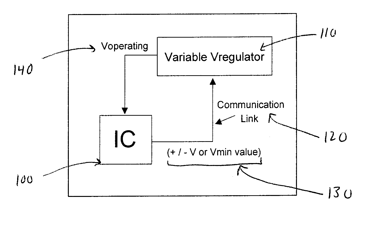
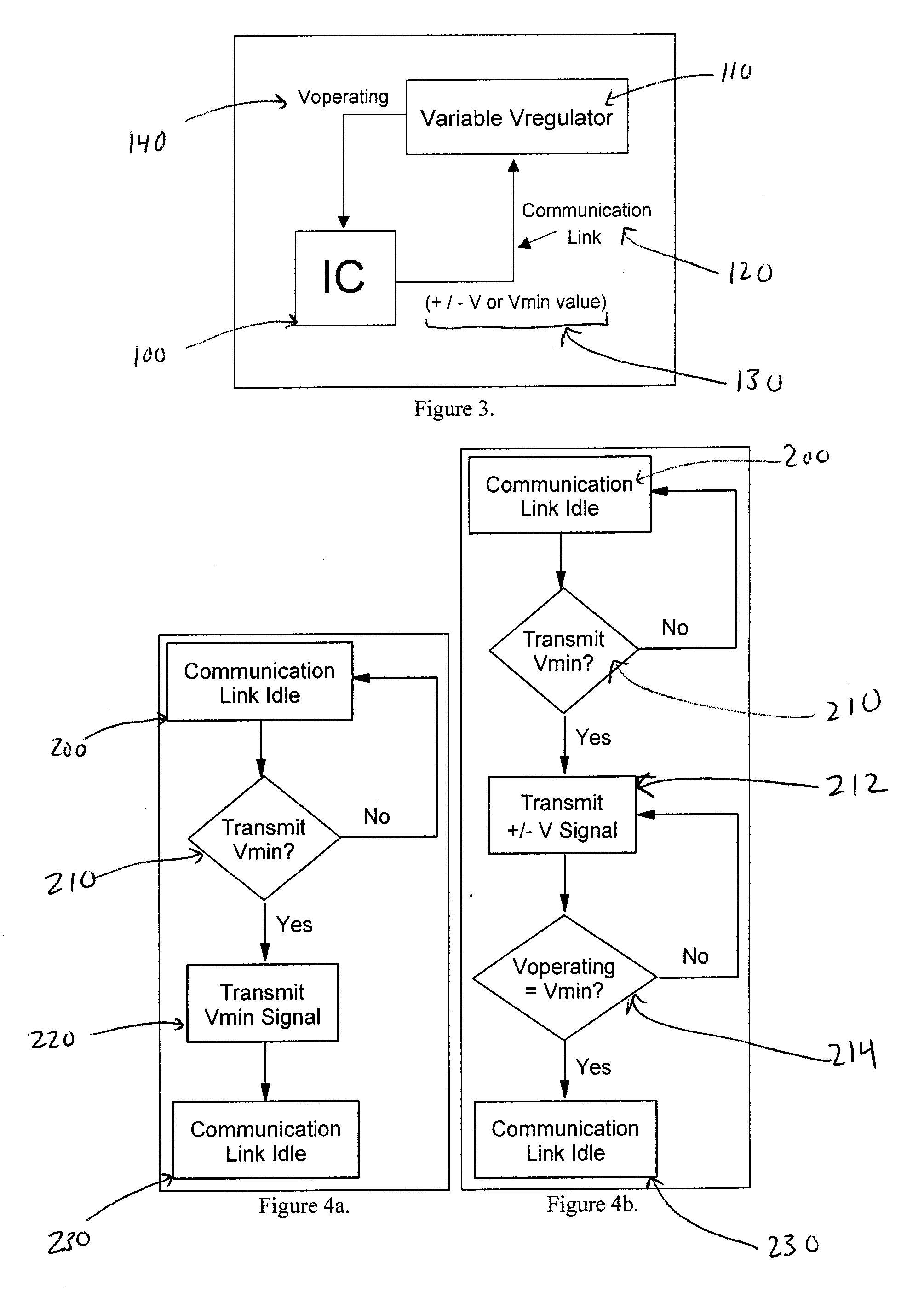
[0048]FIG. 5 illustrates a second embodiment where IC 302 is capable of self-testing, which is performed by a built-in-self-test (“BIST”) engine, so that Vmin may be determined while the IC is in the end system. Preferably, self-testing is performed during IC initialization in order to minimize potential system interruption. This may occur during each IC initialization or may occur at some interval of initializations (e.g. every 10th initialization, self-testing is performed). Self-testing may be performed during normal operating conditions or any other time when the IC is in the end system (e.g. idle state). In addition to optimizing power consumption, this embodiment also provides a means for adjusting the operating voltage of an IC throughout its useful life. As is well know in the art, IC performance degrades over time as a result of reliability wearout mechanisms. For example, IC performance will decrease as a result of hot electron degradation which causes damage at the gate / d...

third embodiment

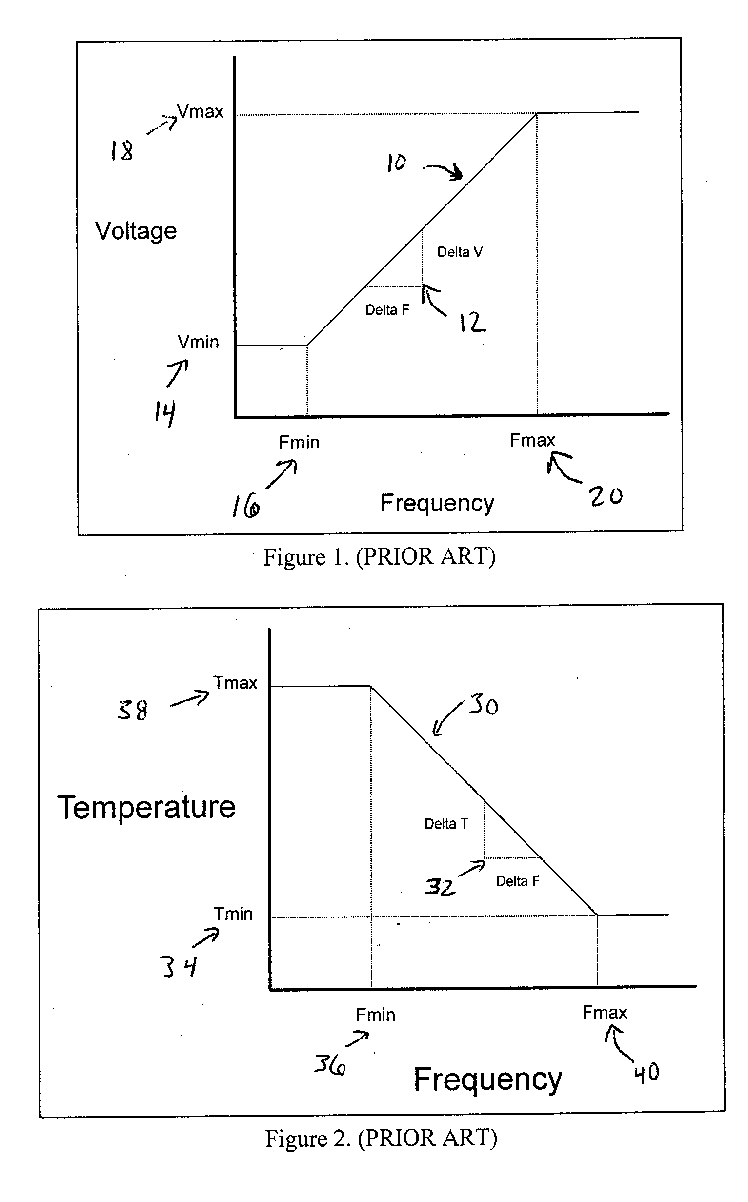
[0058]FIG. 9 illustrates a third embodiment where system temperature may be utilized to reduce the operating voltage of an IC, and thus, power consumption. Because the operating frequency of an IC is inversely related to temperature, an IC tested at worst-case system operating temperature, but which is actually operating at some temperature below that condition, may be operated at a lower voltage and still satisfy the system performance requirements. The end system contains temperature monitoring system 500 (e.g. thermal couple, thermal monitor, etc.) that is capable of measuring the temperature of the system near IC 502 and transmitting that temperature data to the IC for processing 504. In an alternate embodiment, a temperature sensing mechanism is contained within the IC. Techniques for measuring temperature using devices contained within semiconductor circuits are well known and described more fully in U.S. Pat. No. 3,881,181 entitled SEMICONDUCTOR TEMPERATURE SENSOR, by Khajeza...


PUM


Abstract

A method and apparatus for adaptively adjusting the operating voltage of an integrated circuit in response to tester-to-system variations, worst-case testing techniques, process variations, temperature variations, or reliability wearout mechanisms. The minimum operating voltage of an integrated circuit is determined either during external testing of the integrated circuit or during built-in-self-testing. The minimum operating voltage is transmitted to a variable voltage regulator where it is used to set the output of the regulator. The output of the regulator supplies the integrated circuit with its operating voltage. This technique enables tailoring of the operating voltage of integrated circuits on a part-by-part basis which results in power consumption optimization by adapting operating voltage in response to tester-to-system variations, worst-case testing techniques, process variations, temperature variations or reliability wearout mechanisms. Alternatively, the invention enables adaptive adjustment of the operating frequency of an integrated circuit. The invention enables system designers to adaptively optimize either system performance or power consumption on a part-by-part basis in response to tester-to-system variations, worst-case testing techniques, process variations, temperature variations or reliability wearout mechanisms.

Description

BACKGROUND OF INVENTION [0001] The present invention relates to controlling power consumption of an electronic component within an electronic system. Alternatively, the present invention relates to controlling operating frequency of an electronic component within an electronic system. [0002] Power consumption increasingly has become a major obstacle to circuit and system designers. Advances in integrated circuit (IC) technology have resulted in millions of transistors being placed on single ICs. Additionally, IC technology advances also enable circuits to switch at increasingly faster speeds. As the physical sizes of ICs continue to shrink while at the same time performance (i.e. switching speed) increases, power density substantially increases. This substantial increase in power density causes power management problems for system designers. Power management problems take form in both heat dissipation and battery life issues. Greater power dissipated by ICs with ever decreasing area...

Claims


Application Information

Patent Timeline
Patent Type & Authority Applications(United States)
IPC IPC(8): G06F1/26G06F1/32
CPCG06F1/3203G06F1/3284Y02B60/1285Y02B60/1217Y02B60/1267G06F1/3296Y02D10/00
Inventor BILAK, MARK
Owner IBM CORP
Why Eureka
Try Eureka