

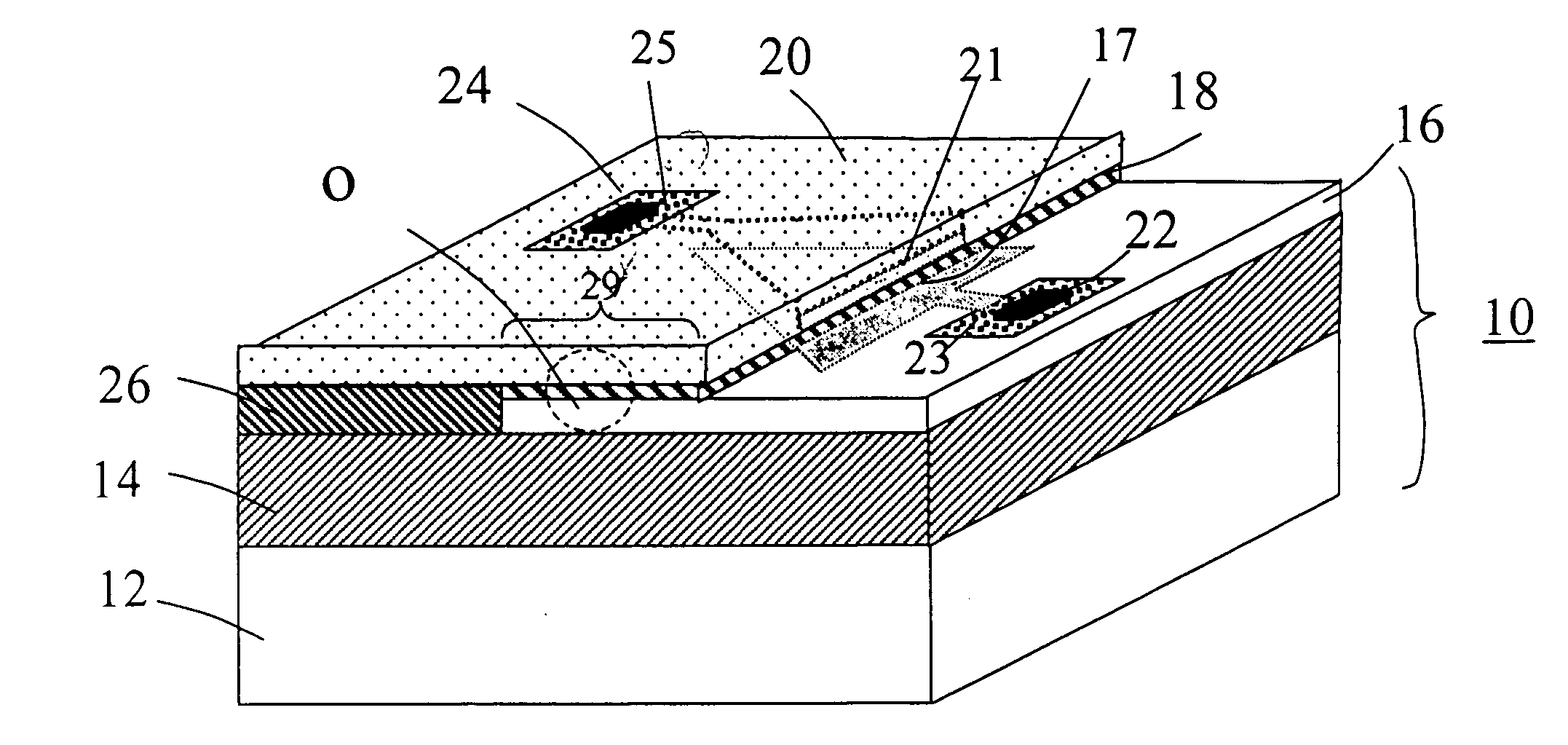
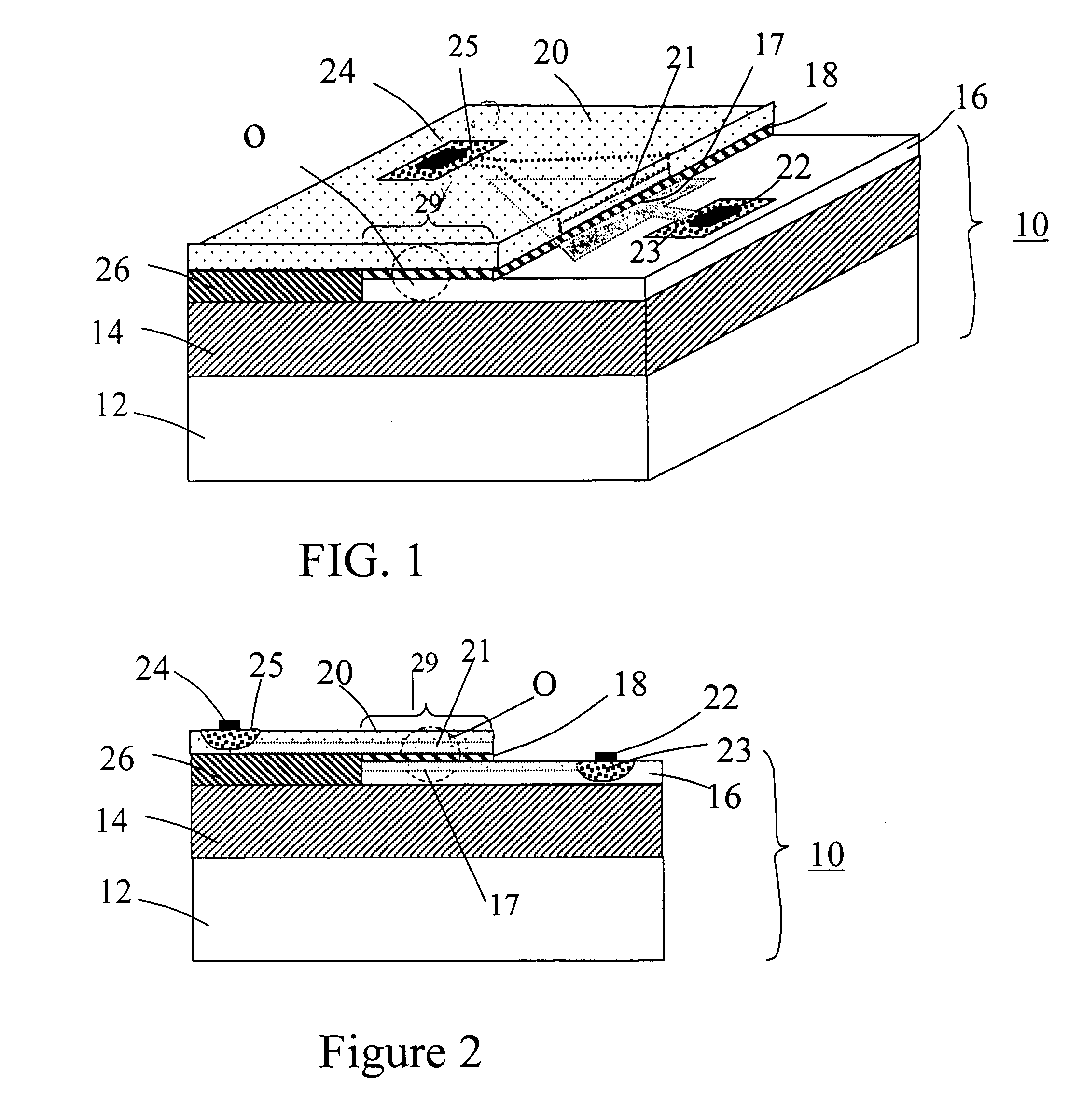
Active manipulation of light in a silicon-on-insulator (SOI) structure
a technology of active manipulation and silicon-on-insulator, which is applied in the direction of instruments, optical elements, optical waveguide light guides, etc., can solve the problems of reducing and affecting the transmission ability of ligh
- Summary
- Abstract
- Description
- Claims
- Application Information
AI Technical Summary
Benefits of technology
Problems solved by technology
Method used
Image

Examples
Embodiment Construction
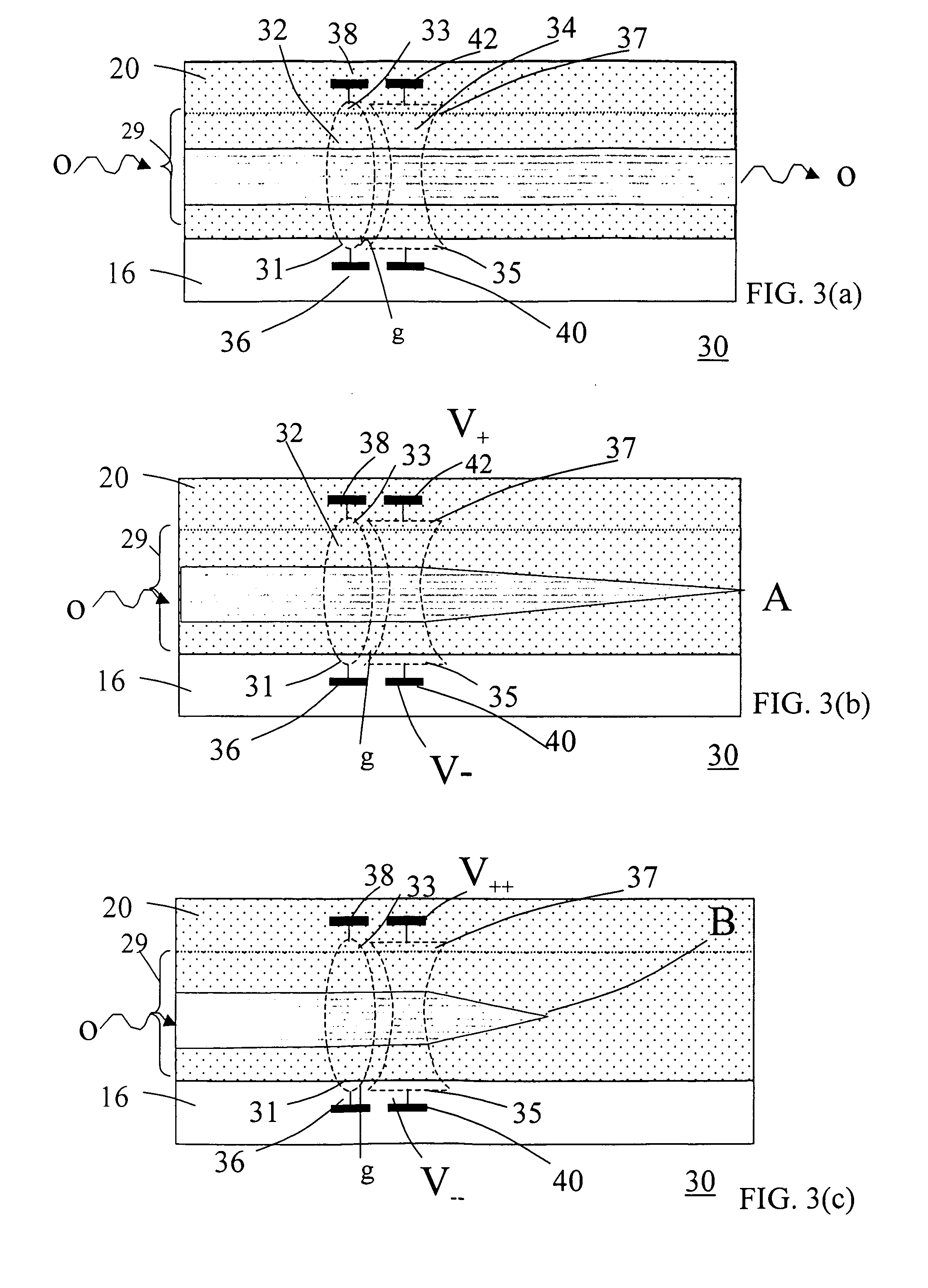
[0025] Unstrained, pure silicon exhibits no linear electro-optic (Pockels) effect, and non-linear effects such as the Franz-Keldysh and Kerr effects are very weak in pure silicon. For the Kerr effect, an applied field in the range of 105 V / cm produces a change in the refractive index on the order of only about 10−8 to 10−5. The most effective mechanisms to vary the refractive index / optical absorption of light in silicon are the free carrier effect (Δn˜10−3) and the thermo-optic effect (Δn˜10−4). The thermo-optic effect is defined as a change in the refractive index due to a change in the temperature of the silicon. The thermo-optic effect is rather slow (on the order of <1 MHz), and finds limited applications in today's high speed communication applications.
[0026] The present invention is based upon the utilization of the free carrier effect in thin SOI (sub-micron) waveguide geometry. The waveguide geometry more particularly utilizes a SISCAP structure comprising a relatively thin...
PUM
 Abstract
Description
Claims
Application Information