Semiconductor device

a semiconductor device and semiconductor technology, applied in the field of semiconductor devices, can solve the problems of increasing affecting the performance of the semiconductor device, and so as to prevent the transmission of noise, prevent the increase of the manufacturing cost of the semiconductor device, and prevent the effect of the noise of the substra

a semiconductor device and semiconductor technology, applied in the field of semiconductor devices, can solve the problems of increasing affecting the performance of the semiconductor device, and so as to prevent the transmission of noise, prevent the increase of the manufacturing cost of the semiconductor device, and prevent the effect of the noise of the substra

US20050189602A1Inactive Publication Date: 2005-09-01RENESAS ELECTRONICS CORP

Image

  • Semiconductor device
  • Semiconductor device
  • Semiconductor device

Examples


Embodiment Construction

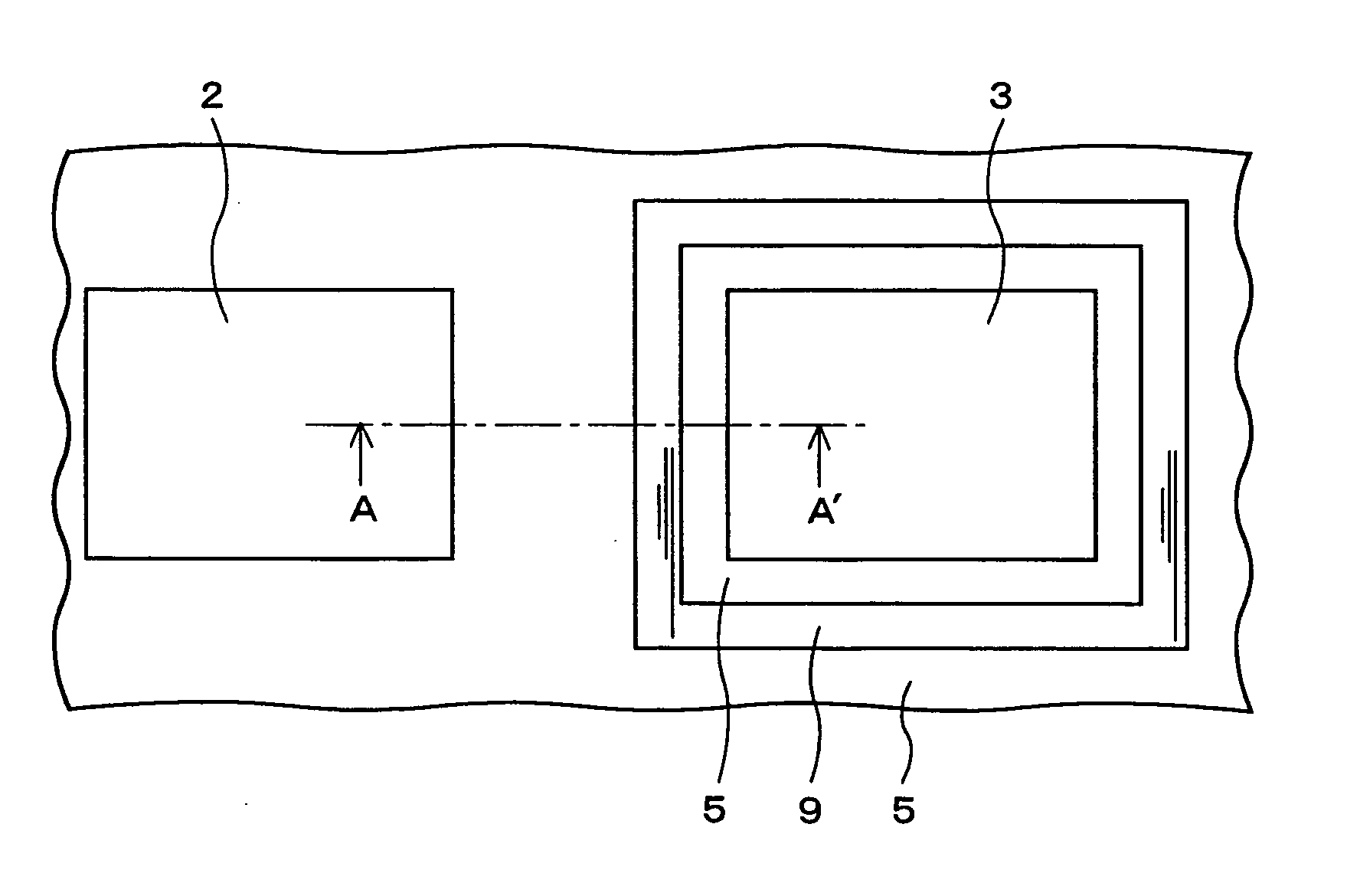
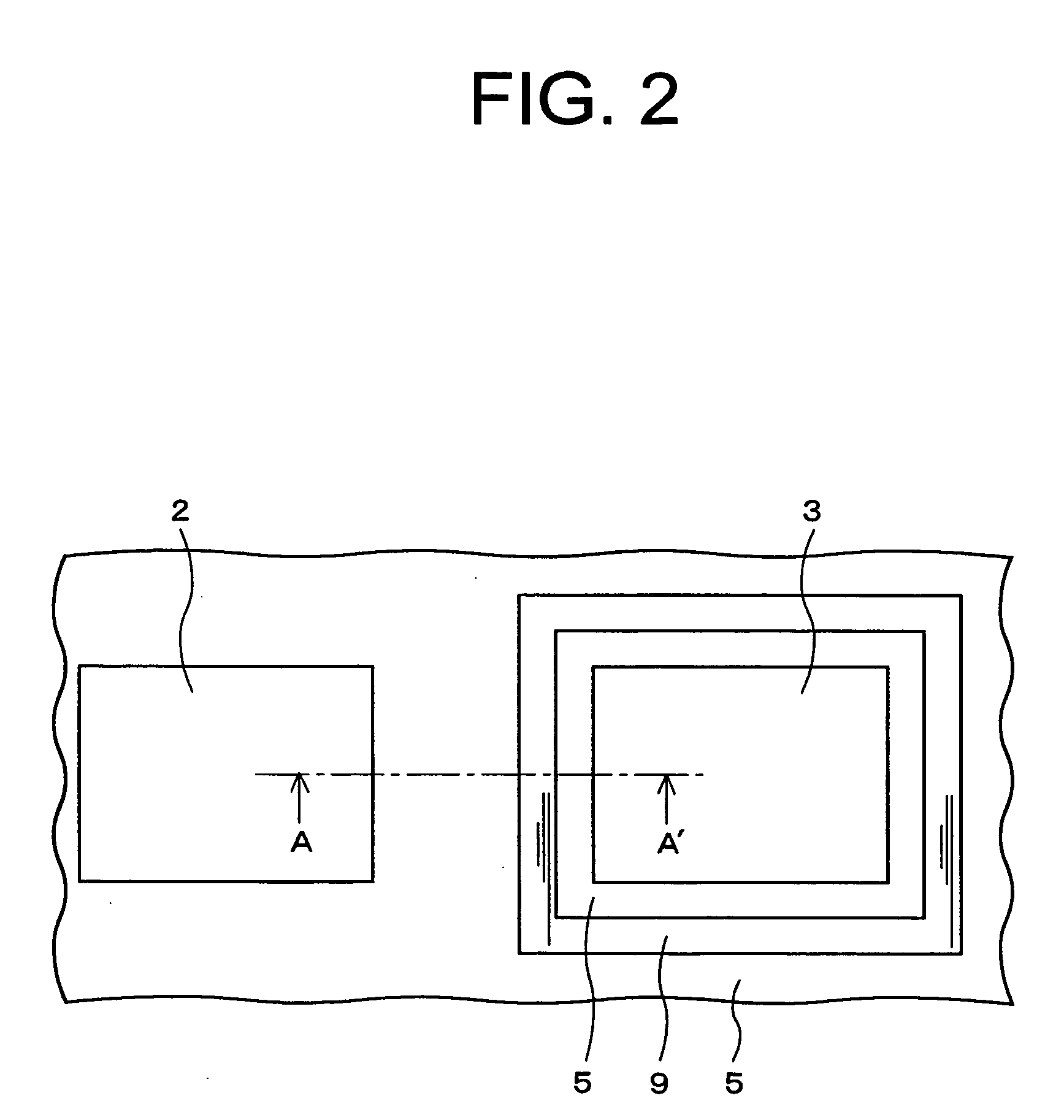
[0023] Now, embodiments of the invention will be described in detail in conjunction with the accompanying drawings. A first embodiment of the invention will be described. FIG. 2 is a plan view of a semiconductor device according to the embodiment, and FIG. 3 is a sectional view taken along the line A-A′ in FIG. 2. As shown in FIGS. 2 and 3, in the semiconductor device according to the embodiment, a p type silicon substrate 1 is provided, and there are circuit regions 2 and 3 formed at the surface of the p type silicon substrate 1. The circuit region 2 has a circuit as a noise source such as a digital circuit. The circuit region 3 has an affected circuit liable to be affected by noise such as an analog circuit and for example a PLL circuit (Phase-Locked Loop circuit) is provided in the region.

[0024] The circuit region 2 has a p+ diffusion region 2a, and the circuit region 3 has a p+ diffusion region 3a. The p+ diffusion regions 2a and 3a are connected to upper layer lines (not shown...


PUM


Abstract

An insulating film is provided in a region surrounding a circuit region on a p type silicon substrate, and a frame-shaped electrode is provided to surround the circuit region on the insulating film. The region directly under the electrode at the surface of the p type silicon substrate is formed as a non-doped region with no impurity implanted. Then, a positive power supply potential is applied to the electrode. In this way, a depletion layer is formed directly under the electrode at the surface of the p type silicon substrate. Consequently, the substrate noise is shielded.

Description

BACKGROUND OF THE INVENTION [0001] 1. Field of the Invention [0002] The present invention relates to a semiconductor device including a guard ring. [0003] 2. Description of the Related Art [0004] There has been a known technique of providing a guard ring around a circuit region formed at the surface of a semiconductor substrate. FIG. 1 is a sectional view of such a conventional semiconductor device including a guard ring. As shown in FIG. 1, in the semiconductor device, circuit regions 102 and 103 are formed at the surface of a p type silicon substrate 101. The circuit region 102 has a circuit as a noise source such as a digital circuit. The circuit region 103 has a circuit liable to be affected by noise such as an analog circuit. The circuit region 102 is provided with a p+ diffusion region 102a, while the circuit region 103 is provided with a p+ diffusion region 103a. Note that in FIG. 1, the elements other than the p+ diffusion regions 102a and 103a in the circuit regions 102 and...

Claims


Application Information

Patent Timeline
01 Sep 2005
Publication
US20050189602A1
IPC
H01L21/761; H01L21/765; H01L21/822; H01L23/58; H01L27/04; H01L21/76; H01L29/00; H01L29/06; H01L29/51; H01L29/74; H01L31/111
CPC
H01L21/761; H01L21/765; H01L29/0619; H01L2924/0002; H01L2924/00
Inventors
YAMAMOTO, RYOTA; NAKASHIBA, YASUTAKA