Apparatus and method for measuring substrates

Inactive Publication Date: 2005-09-01
SAMSUNG ELECTRONICS CO LTD
View PDF3 Cites 70 Cited by
  • Summary
  • Abstract
  • Description
  • Claims
  • Application Information

AI Technical Summary

Benefits of technology

[0008] A substrate contact hole measuring apparatus is provided that efficiently measures property values of a contact hole formed in a material layer of a test substrate by irradiating

Problems solved by technology

Thus, an increase in the resistance value causes a bad electrical connection between the upper and lower conductors.
Typically, contact holes are destructively tested by sawing a wafer to check the vertical profile of the wafer.
The former offers a comparative precision, b

Method used


Image

  • Apparatus and method for measuring substrates
  • Apparatus and method for measuring substrates
  • Apparatus and method for measuring substrates

Examples


Example

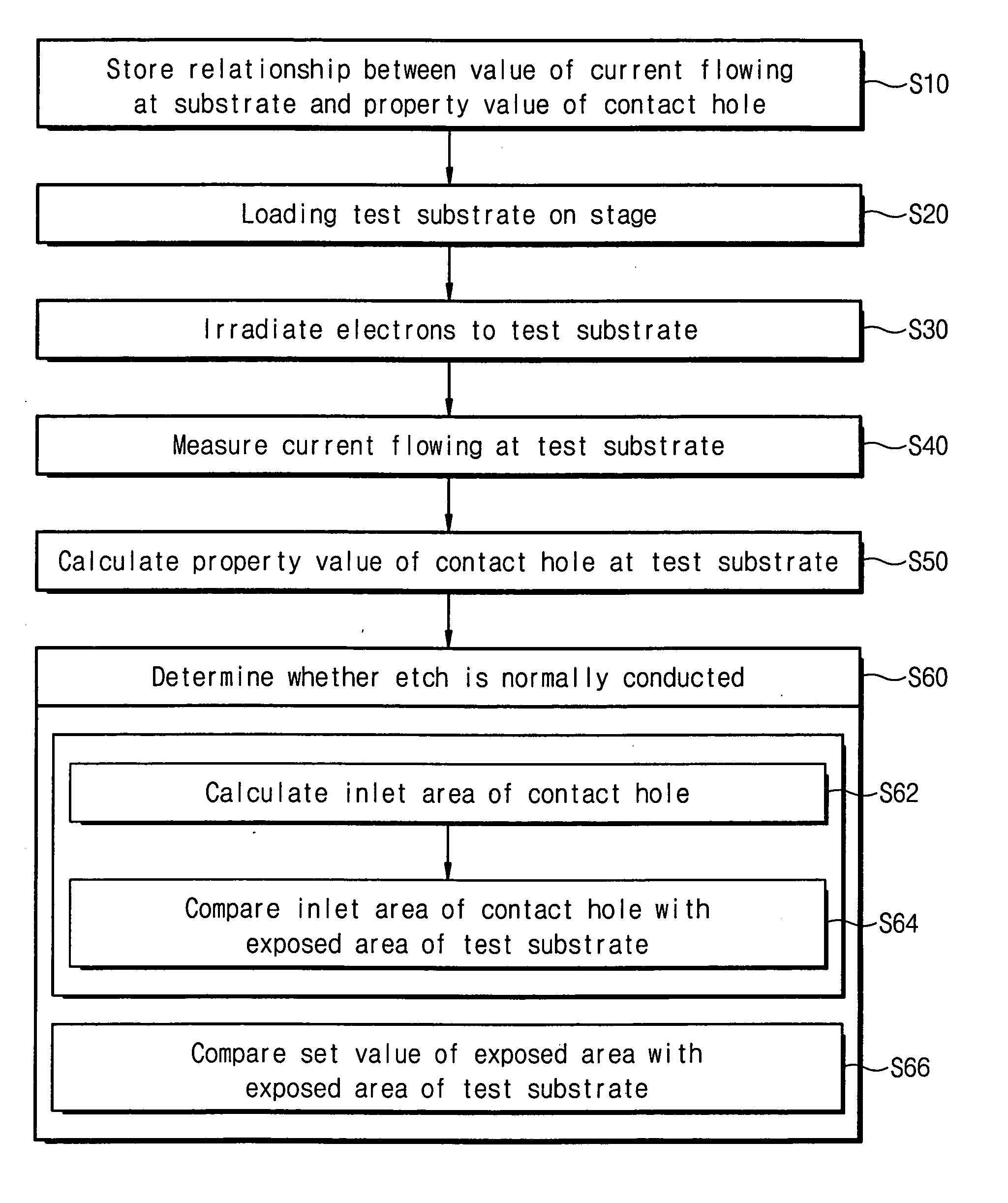
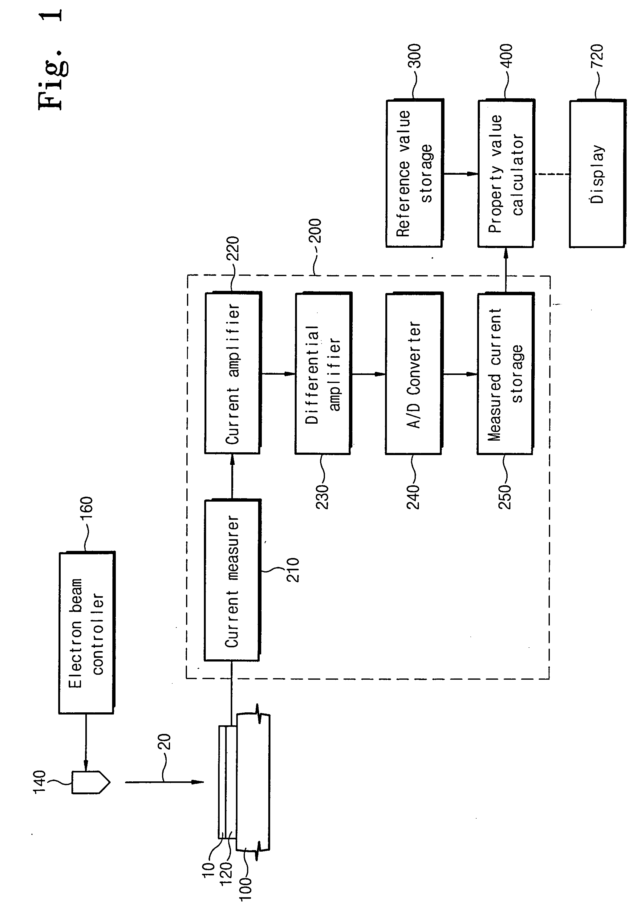
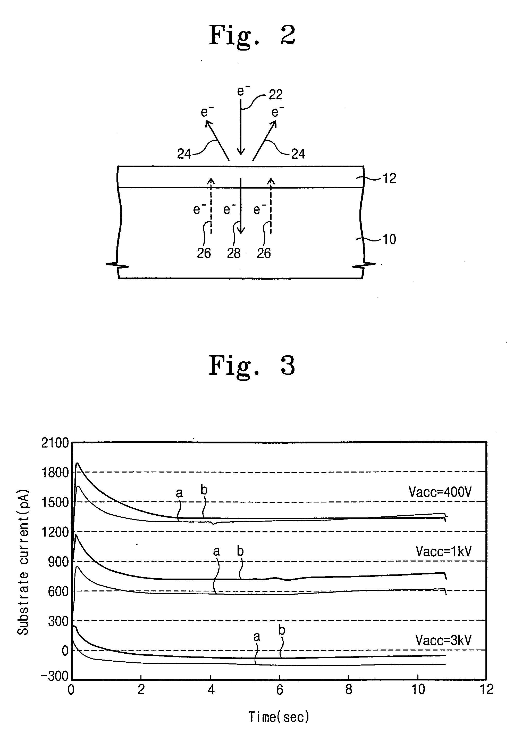
[0040] The present invention will now be described more fully hereinafter with reference to the accompanying drawings, in which preferred embodiments of the invention are shown. The invention may, however, be embodied in different forms and should not be construed as limited to the embodiments set forth herein. Rather, these embodiments are provided so that this disclosure will be thorough and complete, and will fully convey the scope of the invention to those skilled in the art. In the drawings, the height of layers and regions are exaggerated for clarity.

[0041] In this embodiment, a substrate may be a silicon substrate or a substrate on which predetermined layers are deposited. The deposited material layers may be dielectric layers made of, for example, silicon oxide (SiO2), silicon nitride (SiN), silicon oxynitride (SiON), aluminum oxide (Al2O3), hafnium oxide (HfO2), and combinations thereof. A substrate measuring apparatus measures property values of contact holes formed at a ...


PUM


Abstract

A substrate measuring apparatus includes a reference value storage unit, an electron irradiator, a current measuring device, and a property value calculating device. The reference value storage unit stores data on the relationship between current flow in a sample substrate with a contact hole of known characteristics that is irradiated by an electron beam. The current measuring device measures current flow in a test substrate. The property value calculating device calculates the property value of the contact hole formed in a material layer of the test substrate using the current flow in the test substrate and the data stored in the reference value storage unit. The property values of the contact hole may be a surface area of underlying substrate exposed by a contact hole or an amount of residual material remaining in the contact hole.

Description

PRIORITY STATEMENT [0001] This application claims the priority of Korean Patent Application No. 2004-13197, filed on Feb. 26, 2004 in the Korean Intellectual Property Office, the disclosure of which is incorporated herein in its entirety by reference. BACKGROUND OF THE INVENTION [0002] 1. Field of the Invention [0003] The present invention relates to an apparatus and method for measuring substrates and, more particularly, to an apparatus and method for measuring property values of contact holes formed at a material layer on a substrate. [0004] 2. Description of Related Art [0005] In fabrication of semiconductor devices, deposition, exposure, and etching processes are repeatedly performed on a semiconductor substrate such as a silicon wafer to form patterns that have the properties of the semiconductor devices. Such semiconductor devices may require an electrical connection of upper and lower conductors with an interlayer dielectric interposed therebetween. The upper and lower conduc...

Claims


Application Information

Patent Timeline
IPC IPC(8): G01N27/416G01R31/26H01L21/4763H01L21/66H01L21/768
CPCH01L21/76802H01L22/14H01L2924/0002H01L2924/00G01B3/1005G01B2003/1033G01B2003/1076
Inventor YOON, YOUNG-JEEJUN, CHUNG-SAMSONG, CHUL-GICHON, SANG-MUN
Owner SAMSUNG ELECTRONICS CO LTD
Why Eureka
Try Eureka