LED fabrication via ion implant isolation

a technology of ion implant and fabrication process, which is applied in the manufacture of semiconductor/solid-state devices, semiconductor devices, electrical devices, etc., can solve the problems of additional difficulties, the process of die separation may be harmful to the exposed p-n junction region, and the ultra-toughness of led lamps

Inactive Publication Date: 2005-09-08
CREE INC
View PDF41 Cites 39 Cited by
  • Summary
  • Abstract
  • Description
  • Claims
  • Application Information

AI Technical Summary

Problems solved by technology

LED lamps are extremely tough.
Additionally, the passivation layer (typically silicon nitride) that is often added to protect the diode can crack following thermal or mechanical stress and thus provide additional possibilities for the development of undesired contacts to the epitaxial layers of the device.
The process of die separation may be harmful to exposed p-n junction regions.
In particular, when the purpose of the patterning step is to define an etch pattern in a GaN-based layer, GaN's chemical, physical, and thermal stability (which are favorable characteristics in finished devices) can cause additional difficulties if the etchant removes the resist before fully removing the desired pattern of material.

Method used


Image

  • LED fabrication via ion implant isolation
  • LED fabrication via ion implant isolation
  • LED fabrication via ion implant isolation

Examples


Embodiment Construction

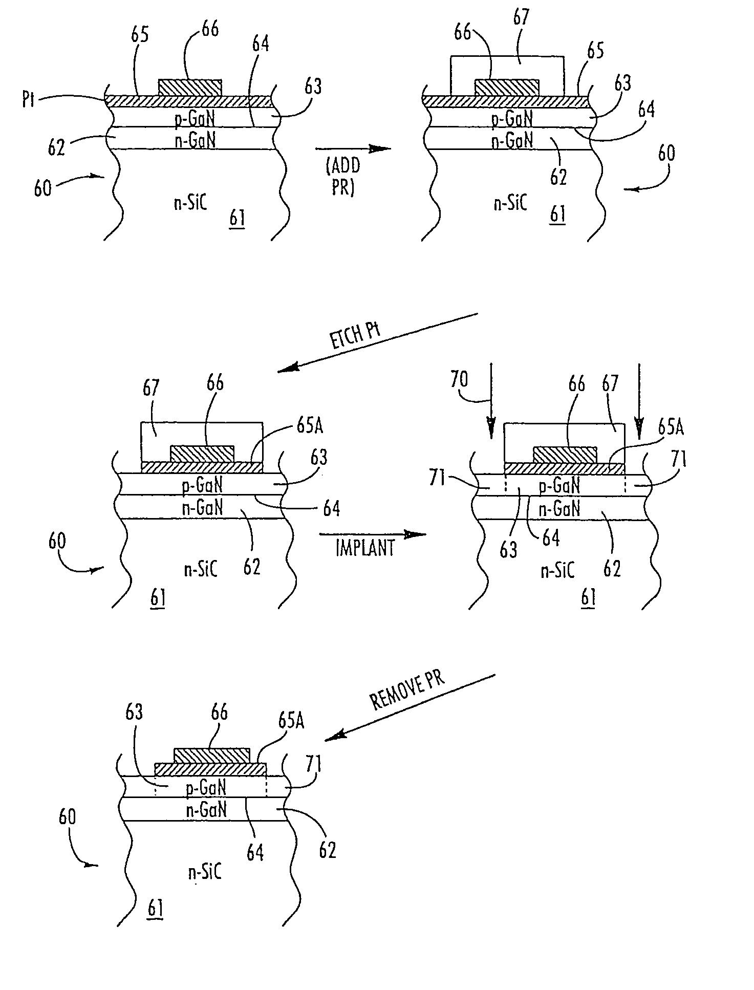
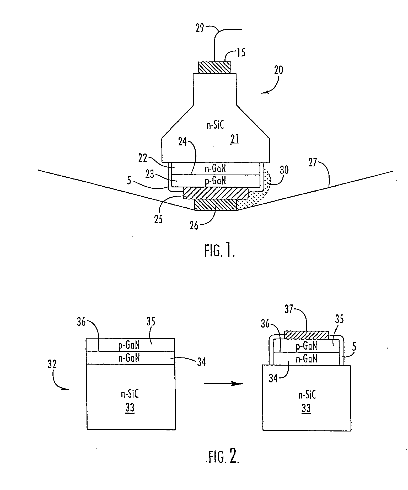
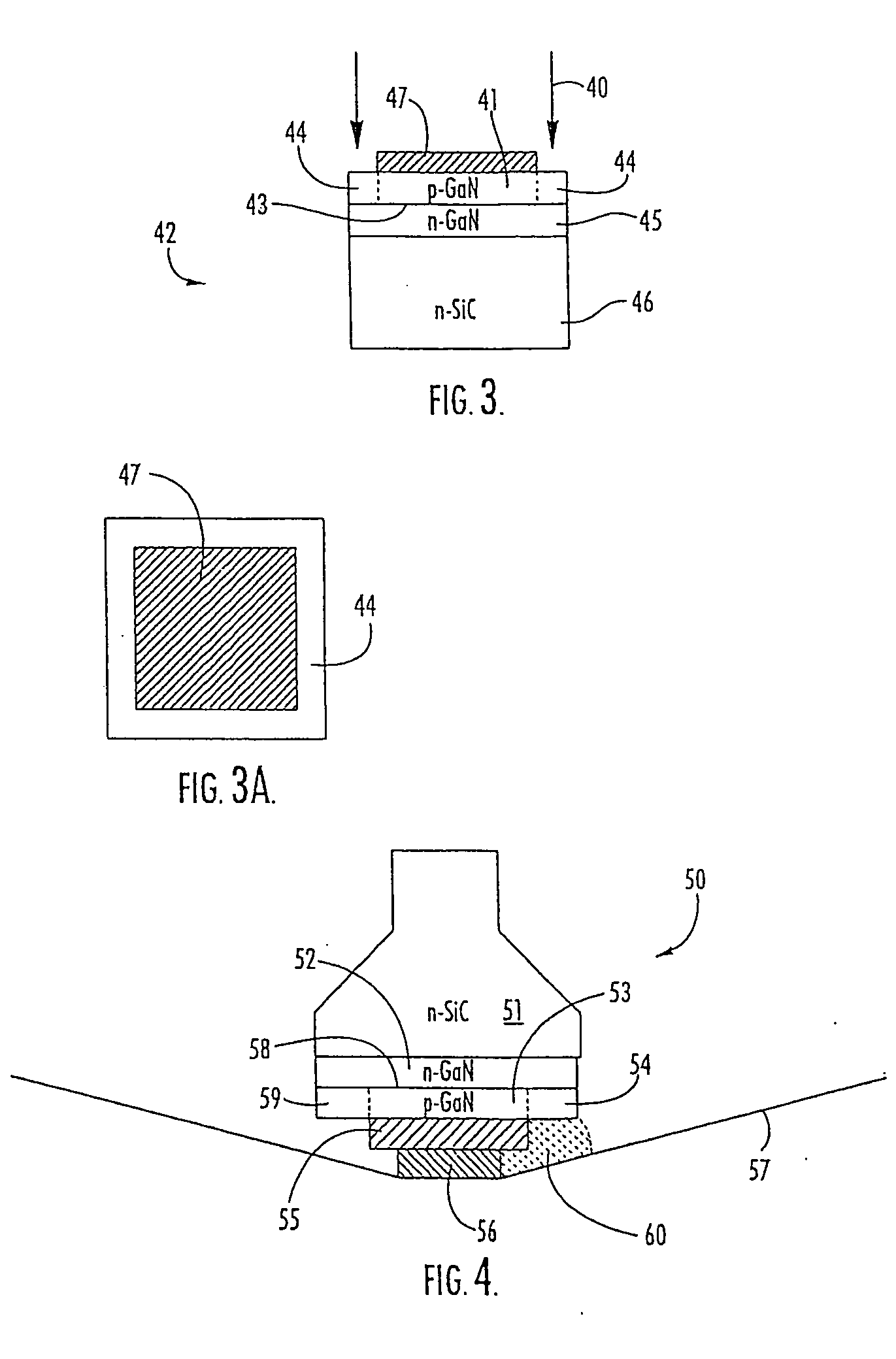
[0028] The present invention now will be described more fully hereinafter with reference to the accompanying drawings, in which preferred embodiments of the invention are shown. This invention may, however, be embodied in many different forms and should not be construed as limited to the embodiments set forth herein; rather, these embodiments are provided so that this disclosure will be thorough and complete, and will fully convey the scope of the invention to those skilled in the art. In the drawings, the thickness of layers and regions are exaggerated for clarity. It will be understood that when an element such as a layer, region or substrate is referred to as being “on” another element, it can be directly on the other element or intervening elements may also be present. In contrast, when an element is referred to as being “directly on” another element, there are no intervening elements present. Moreover, it will be understood that when a first element or layer is described as “in...


PUM


Abstract

A semiconductor light emitting diode includes a semiconductor substrate, an epitaxial layer of n-type Group III nitride on the substrate, a p-type epitaxial layer of Group III nitride on the n-type epitaxial layer and forming a p-n junction with the n-type layer, and a resistive gallium nitride region on the n-type epitaxial layer and adjacent the p-type epitaxial layer for electrically isolating portions of the p-n junction. A metal contact layer is formed on the p-type epitaxial layer. Some embodiments include a semiconductor substrate, an epitaxial layer of n-type Group III nitride on the substrate, a p-type epitaxial layer of Group III nitride on the n-type epitaxial layer and forming a p-n junction with the n-type layer, wherein portions of the epitaxial region are patterned into a mesa and wherein the sidewalls of the mesa comprise a resistive Group III nitride region for electrically isolating portions of the p-n junction. In method embodiments disclosed, the resistive border is formed by forming an implant mask on the p-type epitaxial region and implanting ions into portions of the p-type epitaxial region to render portions of the p-type epitaxial region semi-insulating. A photoresist mask or a sufficiently thick metal layer may be used as the implant mask. In some method embodiments, a mesa is formed in the epitaxial region prior to implantation. During implantation, the epiwafer is mounted at an angle such that ions are implanted directly into the sidewalls of the mesa, thereby rendering portions of the mesa semi-insulating. The epiwafer may be rotated during ion implantation.

Description

[0001] This application claims priority from application No. 60 / 519,197 filed Nov. 12, 2003 for “LED Fabrication via Ion Implant Isolation.”BACKGROUND OF THE INVENTION [0002] The present invention relates to the manufacture and packaging of semiconductor light emitting diodes (“LED”). An LED is a semiconductor device that emits light whenever current passes through it. In its simplest form, a light emitting diode includes a p-type portion and an n-type portion to define a p-n junction diode. When mounted on a lead frame and encased in an encapsulant (usually a polymer), the overall LED package is also referred to as a “lamp.”[0003] Because of the high reliability, long life and generally low cost of LEDs, they have gained wide acceptance in a variety of lighting applications in many fields of application. [0004] LED lamps are extremely tough. They typically do not include glass and avoid filaments entirely. As a result, LED lamps can take abuse far beyond that of the incandescent la...

Claims


Application Information

Patent Timeline
Patent Type & Authority Applications(United States)
IPC IPC(8): H01L29/06H01L31/0328
CPCH01L21/2654H01L33/025H01L33/44H01L33/24H01L33/32H01L33/145H01L2224/32245H01L2224/48091H01L2224/48247H01L2224/73265H01L2924/00014H01L2924/00
Inventor SLATER, DAVID BEARDSLEY JR.EDMOND, JOHN ADAMSUVOROV, ALEXANDERHAMILTON, IAIN
Owner CREE INC
Why Eureka
Try Eureka