
Eureka
For R&D, Eureka makes reading and utilizing patents & technical documents easy.
Eureka AIR
Designed for self-driven R&D workflows. Generate viable solutions, solve complex R&D challenges, empower your innovation with AI.

Eureka Materials
Designed for material experts only. Revolutionize your material R&D, from search, analyze, to developing new materials.

TechResearch
Generate reliable direction feasibility study reports for your R&D in just a few steps.

TechSeek
Discover and master advanced knowledge NOW. Basics, ideas, possibilities, all at once.

TechMind
As an expert in R&D Theories, TechMind can generates customized viable solutions instantly.

TechRisk
Analyze your overall solution with one click, know your potential R&D risks in advance.

TechMonitor
Get weekly tech updates, stay abreast of the latest tech innovations and key insights.
Optical detection device
- Summary
- Abstract
- Description
- Claims
- Application Information
AI Technical Summary
Problems solved by technology
Method used
Image

Examples
first embodiment
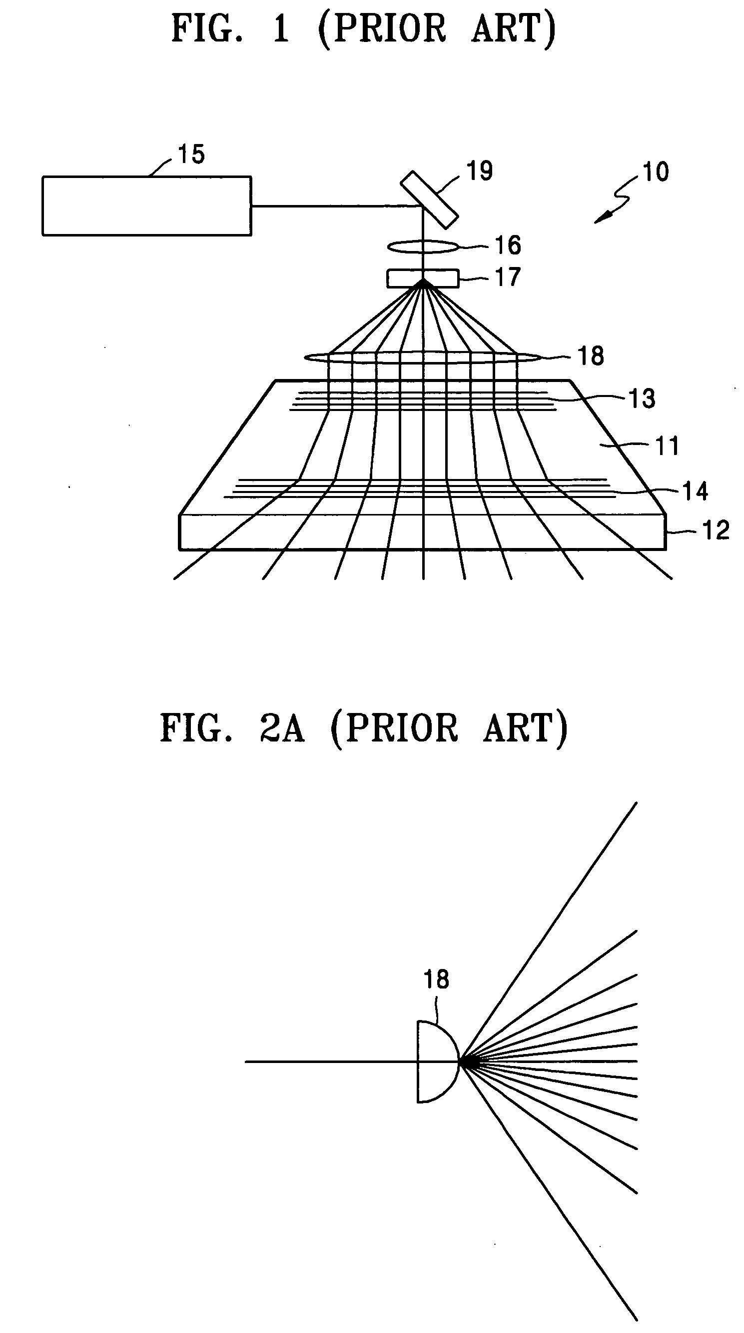
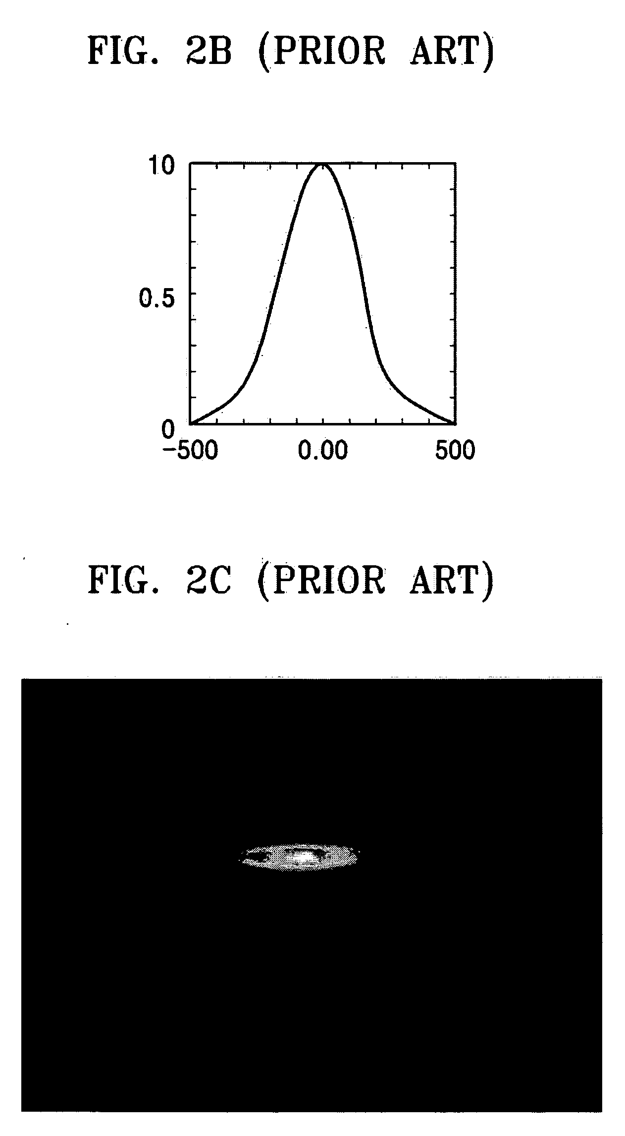
[0036]FIG. 4A is a perspective view of the linear symmetry lens 110 according to the present invention. FIG. 4B is a graph showing an intensity profile of the excitation light having passed through the linear symmetry lens 110 of FIG. 4A. FIG. 4C is a photograph of the excitation light having passed through the linear symmetry lens 110 of FIG. 4A.
[0037] Referring to FIGS. 4A through 4C, the linear symmetry lens 110 according to the first embodiment of the present invention is adapted to focus incident light in one direction but not in the perpendicular direction. Consequently, the excitation light having passed through the linear symmetry lens 110 has a flat line segment-shaped cross-section, as shown in FIG. 4C.
[0038] The linear symmetry lens 110 according to the first embodiment of the present invention is adapted such that excitation light passing through the linear symmetry lens has a uniform intensity distribution, as shown in FIG. 4B.
second embodiment
[0039]FIG. 5 is a perspective view of a linear symmetry lens 210 according to the present invention.
[0040] Referring to FIG. 5, the linear symmetry lens 210 has a function and role substantially similar to the linear symmetry lens 110 according to the first embodiment of the present invention, except that the linear symmetry lens 210 has a convex shape.
[0041] Alternatively, although not shown in the drawings, the linear symmetry lens may have an index of refraction that varies with position in the lens, in order to form a beam with the shape shown in FIGS. 4B and 4C.
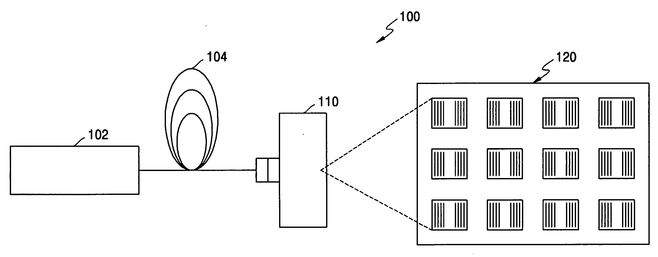
[0042] Referring again to FIG. 3, the flat beam of excitation light having a uniform intensity transmitted through the linear symmetry lens 110 is incident on the detection plate array 120.
[0043]FIG. 6 is a perspective view of the detection plate array 120 with microfluidic chips mounted thereon. FIG. 7 is a schematic diagram depicting excitation light incident on a microfluidic chip mounted on a single detection plat...
PUM
 Abstract
Description
Claims
Application Information
 - R&D Engineer
- R&D Manager
- IP Professional
- Industry Leading Data Capabilities
- Powerful AI technology
- Patent DNA Extraction
Browse by: Latest US Patents, China's latest patents, Technical Efficacy Thesaurus, Application Domain, Technology Topic, Popular Technical Reports.
© 2024 PatSnap. All rights reserved.Legal|Privacy policy|Modern Slavery Act Transparency Statement|Sitemap|About US| Contact US: help@patsnap.com