
Methods and systems for processing microscale devices for reuse

a microfluidic chip and micro-scale technology, applied in the field of systems and methods for reprocessing analytical system components for reuse, can solve the problems of high manual washing difficulty, high cost of chips and waste generation in large microfluidic assay projects, and impracticality in reusing microchips, and achieve high degree of efficiency and effect of effective flushing and washing wells

Active Publication Date: 2005-01-27
CAPLIPER LIFE SCI INC +1
View PDF9 Cites 93 Cited by
  • Summary
  • Abstract
  • Description
  • Claims
  • Application Information

AI Technical Summary

Benefits of technology

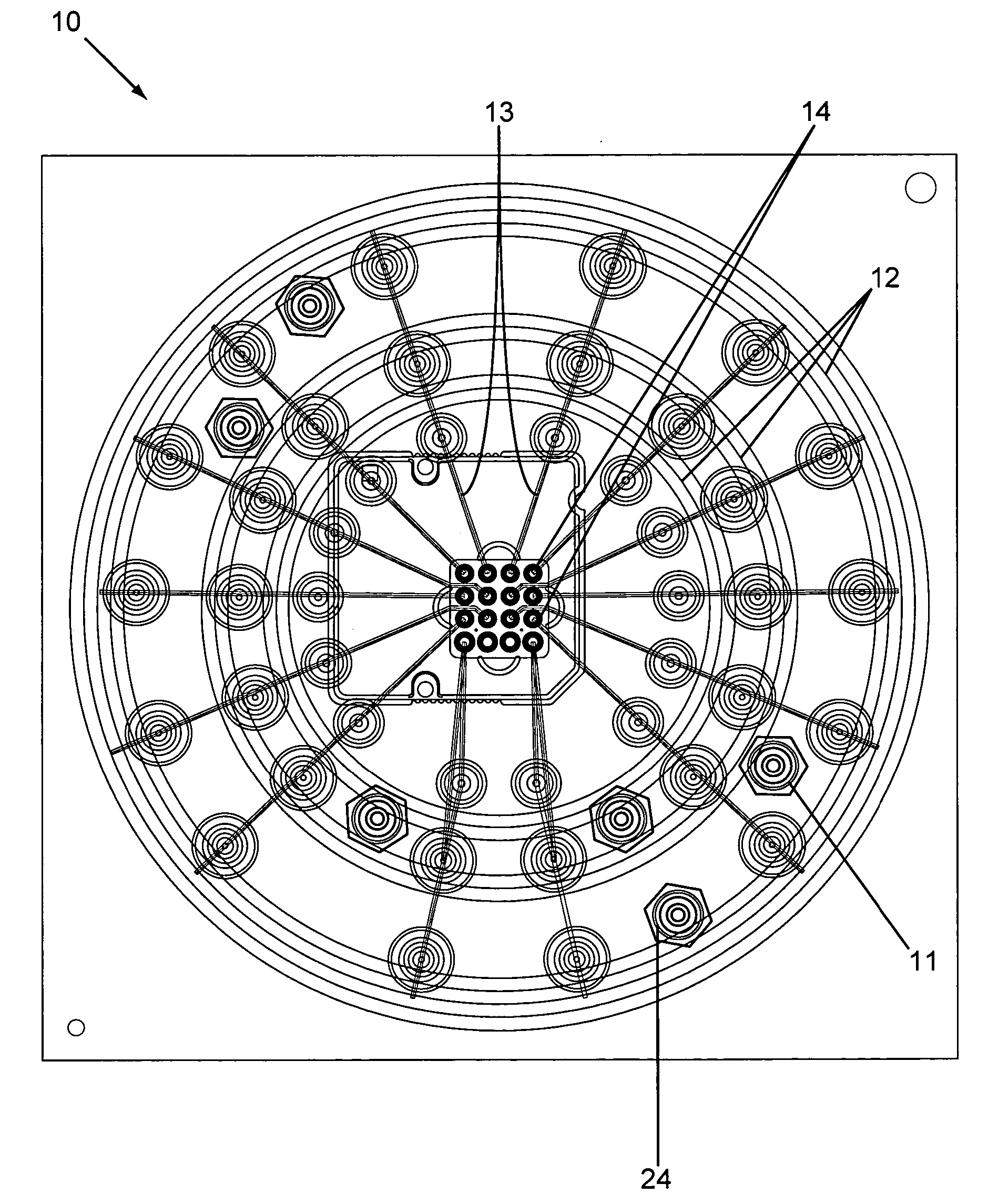
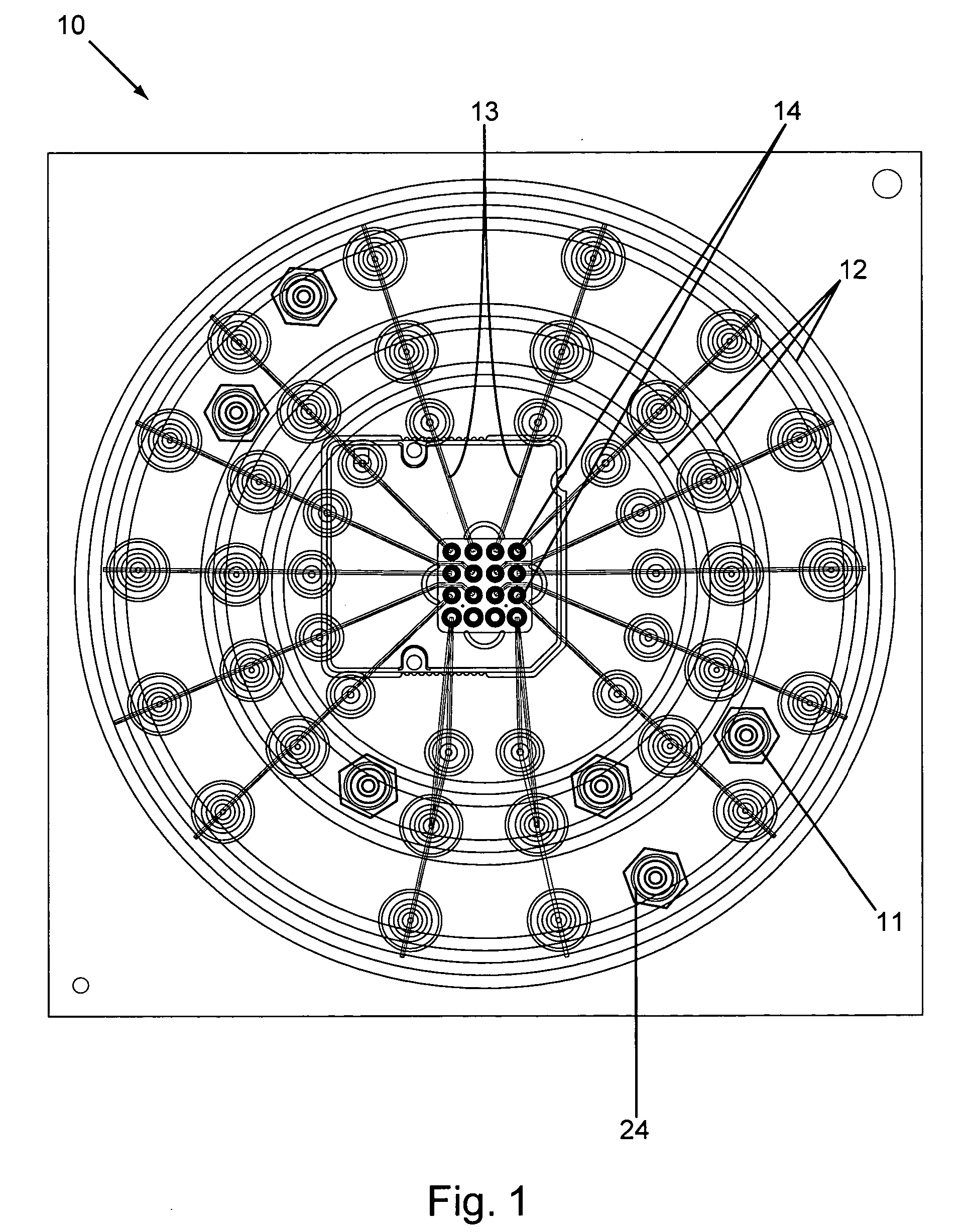
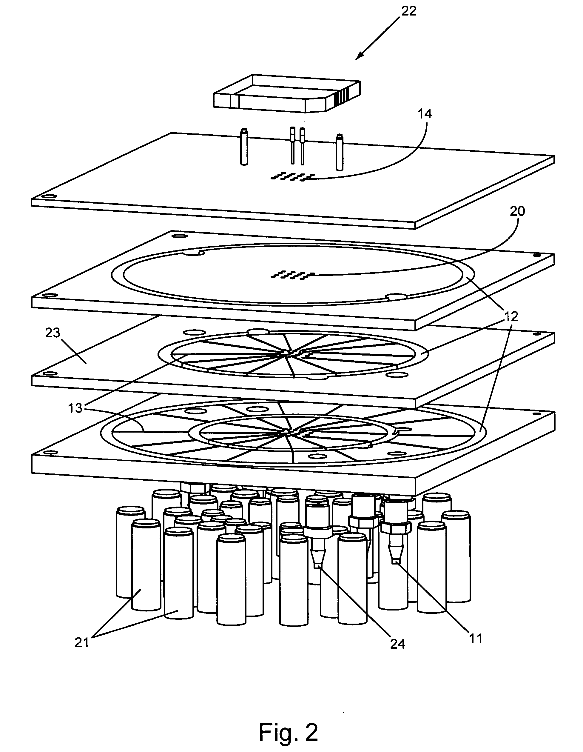
[0019] The present invention includes methods for processing microscale devices for use or reuse. For example, the invention includes methods of processing a microscale device by providing a manifold with one or more mesoscale flush channels or mesoscale waste channels, providing orifices in fluid contact with the flush channels or waste channels and adapted to functionally contact wells of the microscale device, contacting the wells with the orifices, and flowing one or more process solutions through the flush channels into the wells to process the wells and / or one or more microchannels of the microscale device. In preferred embodiments, wells and microchannels of a microscale device are washed with wash solutions and primed with analytical reagents from flush channels of a manifold before reuse of the device. Microscale devices can be effectively processed for use 5 times, 10 times, 20 times, 30 times, or more using methods of the invention.
[0024] Providing orifices adapted to functionally contact the wells in the methods of the invention can include, e.g.: providing 0-rings between the orifices and wells, providing tapered well walls, providing tapered orifices fitted to well walls, or providing a waste channel flow adequate to prevent overflow of process solutions from the wells. In a preferred embodiment, O-rings fitting between the orifices and well walls form a seal capable of transmitting pressure differentials between the manifold and a microscale device. In one embodiment, an orifice is sealed to a well and solutions or gasses under pressure can be directed to flow from the orifice and out of the well alternately through a waste channel of the manifold or through a microchannel of the microscale device. In such a case, the flow of the pressurized solution or gas can be optionally be directed to the microscale channels by closing a control valve in an alternate outlet mesoscale waste channel. In another aspect, gasses or process solutions can flow through one or more radial jets in the orifices to increase the efficiency of well wall flushing.
[0026] Control systems can flexibly control flows of multiple solutions to multiple wells with precise timing. In an aspect of the invention, the flow in the flush channels or the waste channels can be controlled so that two or more wells receive: a different amount of process solution, a different type of process solution, different flushing gas flows, and / or a process solution at a different time.
[0028] Methods of the invention can effectively flush and wash wells and microchannels of a microscale device. Assay solutions, such as test samples or analytical reagents, can be cleared from well and channel volumes and surfaces to a high degree of efficiency. For example, processing a microscale device using methods of the invention can reduce an analyte in wells, and / or in microscale channels, by a million-fold or to less than 1 part per million (ppm). DEFINITIONS

Problems solved by technology

Microfluidic chips are generally disposable devices due to the problems presented in reprocessing them for repeated use.
Reuse of microchips can be impractical because of handling problems, buildup of reagent constituents in the chips, and the introduction of other variables with repeated use that can cause inconsistent results.
However, the cost of chips and the generation of waste in large microfluidic assay projects can add up to a significant expense.
Nevertheless, manual washing can be highly problematic.
However, problems often arise due to the uncontrolled environment and inconsistency of manual procedures.
For example, particles in the environment can enter the chip and clog microchannels, bubbles can be unintentionally introduced into the chip, and use of reagents and accumulation of hazardous wastes can be excessive.
Inconsistent manual processing can result in difficulty validating procedures and low confidence in results.
The time, effort and expense of manual microfluidic chip reprocessing can be prohibitive.
Careful records should be maintained regarding the identification and use of reprocessed microfluidic chips so that the usable life of the chips is not unintentionally exceeded, possibly resulting in corruption of analytical results.
For example, a user may simply fail to record a use.
Also, an identification label affixed to the surface of the microfluidic chip may become lost or illegible due to wet storage of the microfluidic chip, resulting in an inability to identify the microfluidic chip.
If an identification label is affixed to the package for storing the microfluidic chip, the wrong device may be placed into the package.

Method used


Image

  • Methods and systems for processing microscale devices for reuse
  • Methods and systems for processing microscale devices for reuse
  • Methods and systems for processing microscale devices for reuse

Examples


example 1 -

Example 1-A Microfluidic Cartridge Reprocessing System

[0117] In this example, a stand alone processing system includes: a personal computer interacting with air pressure controllers and solenoid valves through a digital I / O interface; pressurized reagent bottles (containers) connected to the air pressure controllers and feeding solutions to ring reservoirs of a manifold through solution supply ports and solution supply control valves; the solenoid valves controlling the flow of house pressurized air to pneumatic valves operatively mounted to the manifold; and, solutions flowing from the ring reservoirs through mesoscale channels in the manifold past open pneumatic valves to orifices arrayed on the surface of the manifold.

[0118] The manifold is mounted on a swing arm above a stage adapted to hold a microscale device in a predetermined orientation. The microscale device is a microfluidic cartridge including a RFID tag data storage module mounted in a mounting plate. After the cartrid...

example 2 -

Example 2-Reuse of a Microscale Device

[0123] Repeated AFP analyses were run on the same sample repeatedly using the same microfluidic cartridge after washing with a processing system (washing fixture) of the invention. The AFP analysis is a liquid phase binding alpha-fetoprotein (AFP) assay involving reaction and binding on-chip of AFP to two antibodies (WA-1 and IgG) which bind to different sites of the protein. The WA-1 antibody is conjugated to a DNA molecule that carries fluorescent labels (Alexa) for the detection. The different complexes and products of the reaction are separated under the influence of an electric field in a separation channel that contains a polymeric matrix (size selective media), and appear at a detector at different times based on their mobility. A typical electropherogram of the assay in 10% serum conditions is shown in FIG. 11.

[0124] The method of the experiment is briefly outlined, as follows: [0125] 1) Fill the cartridge chip on washing fixture with 1...


PUM


Abstract

This invention provides methods and systems for flushing, washing, and priming microscale devices for reuse. Washing and priming methods include flowing solutions from a manifold to flush wells and microchannels of a microfluidic chip. Systems include manifolds adapted to seal and flow solutions or gasses into chip wells. Devices include microfluidic devices with data storage modules to track the reprocessing status of the microscale devices.

Description

CROSS REFERENCE TO RELATED APPLICATIONS [0001] This application claims priority to and benefit of a prior U.S. Provisional Application No. 60 / 546,593, “Methods and Systems for Processing Microscale Devices for Reuse”, by Kechagia et al., filed Feb. 20, 2004, and to prior Provisional Application No. 60 / 492496, “Use of Cleansers to Recondition Microfluidic Chips,” by Rulison, filed Aug. 4, 2003. The full disclosure of the prior applications are hereby incorporated by reference in their entirety.FIELD OF THE INVENTION [0002] The present invention is in the field of systems and methods for reprocessing analytical system components for reuse. In particular, the invention provides systems and methods for flushing, washing, and reusing microfluidic chips. BACKGROUND OF THE INVENTION [0003] Microfluidic chips are generally disposable devices due to the problems presented in reprocessing them for repeated use. Reuse of microchips can be impractical because of handling problems, buildup of re...

Claims


Application Information

Patent Timeline
IPC IPC(8): B01L3/00B01L9/00B01L99/00B81B1/00G01N1/40G01N27/447
CPCB01L3/5027B01L3/502715B01L9/527B01L2300/022B01L2300/024B01L99/00B01L2400/0487G01N1/40G01N27/44704G01N27/44773G01N27/44791B01L2400/0415B01L13/02
Inventor KECHAGIA, PERSEFONIGREENSTEIN, MICHAELBROGDEN, BRUCEDONLON, EDHAYASHI, MASAYOSHIRULISON, AARON J.
Owner CAPLIPER LIFE SCI INC
Learn More