

Methods for forming a semiconductor structure
a technology of semiconductor structure and semiconductor layer, applied in the direction of semiconductor/solid-state device manufacturing, basic electric elements, electric apparatus, etc., can solve the problems of providing a satisfactory solution, and reducing the strength of the bonding layer, so as to minimize surface roughness and improve the bonding strength
- Summary
- Abstract
- Description
- Claims
- Application Information
AI Technical Summary
Benefits of technology
Problems solved by technology
Method used
Image

Examples
Embodiment Construction
[0023] Presented are example embodiments of methods according to the invention, as well as applications based on the transfer of layers using the SMART-CUT® method with Type IV materials or alloys, and in particular with Si and SiGe.
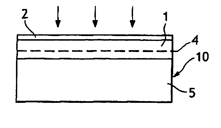
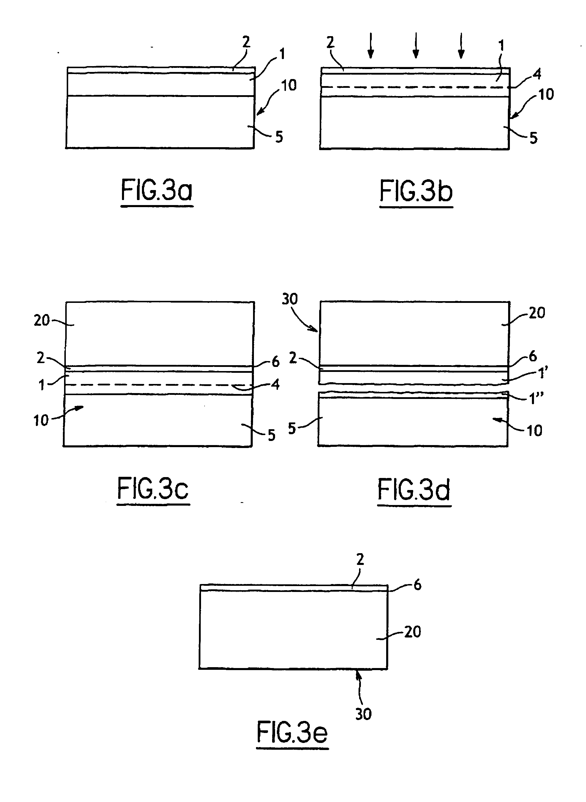
[0024]FIGS. 3a to 3e illustrate a first method for transferring a first layer 1 of Si1-xGex (where x⊖[0;1]) and a second layer 2 of elastically strained Si from a donor wafer 10 to a host wafer 20. FIG. 3a shows a donor wafer 10 that includes the first layer 1 made of Si1-xGex and the second layer 2 made of elastically strained Si. Classically, a donor wafer 10 including Si1-xGex comprises a solid Si substrate 5 on which a buffer structure of SiGe has been formed, for example by crystalline growth, that is made up of different layers. In particular, the buffer structure may be fabricated to have a gradual increasing amount of Ge, starting from 0% at the level of the solid Si substrate to about 100% at the level of the interface with the first layer 1 ma...
PUM
 Abstract
Description
Claims
Application Information