
Light emitting device of III-V group compound semiconductor and fabrication method therefor

a technology of compound semiconductor and light emitting device, which is applied in the direction of semiconductor devices, basic electric elements, electrical apparatus, etc., can solve the problems of restricted light extraction from the light emitting device, and achieve the effect of improving the efficiency of external light extraction

Active Publication Date: 2005-09-15
SHARP KK
View PDF6 Cites 41 Cited by
  • Summary
  • Abstract
  • Description
  • Claims
  • Application Information

AI Technical Summary

Benefits of technology

[0010] In view of the above-described situations of the prior art, an object of the present invention is, in a light emitting device that is fabricated using III-V group compound semiconductor and is capable of emitting blue or white light, to control emission characteristics of the light emitting device while improving efficiency of externally extracting light therefrom.

Problems solved by technology

As such, in the case that molding is carried out after dividing a wafer including the semiconductor layers into chips, extraction of light from the light emitting device is restricted with the emission characteristics dependent on the device structure.

Method used


Image

  • Light emitting device of III-V group compound semiconductor and fabrication method therefor
  • Light emitting device of III-V group compound semiconductor and fabrication method therefor
  • Light emitting device of III-V group compound semiconductor and fabrication method therefor

Examples


first embodiment

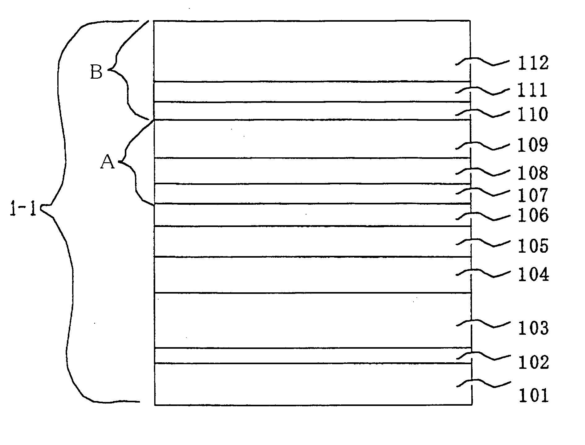
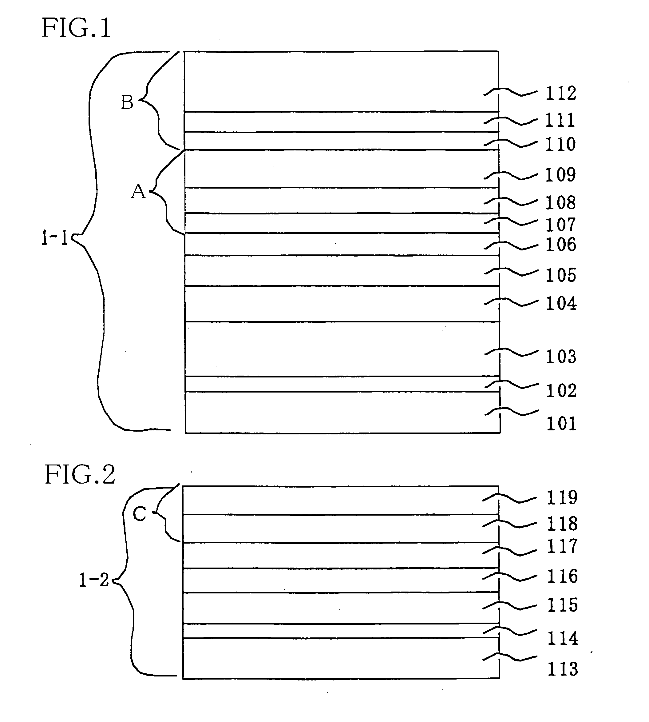
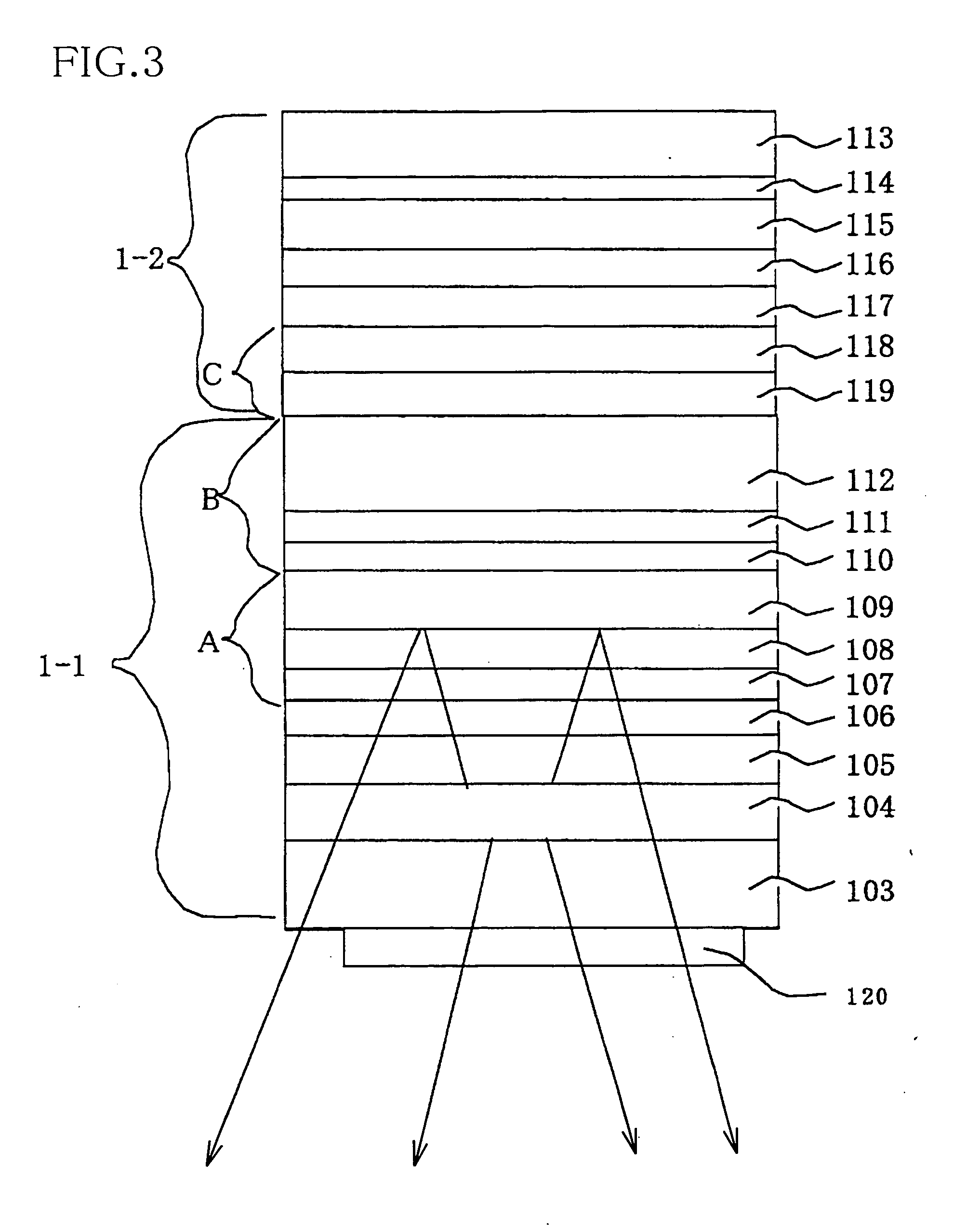
[0030]FIG. 3 shows, in schematic cross section, a light emitting device of III group nitride semiconductor according to a first embodiment of the present invention. In this light emitting device, a transparent n-electrode 120 is formed on a lower surface of a stack 1-1 including a plurality of III group nitride semiconductor layers including a light emitting layer. Bonded on a multiple metal bonding-layer B at the upper side of stack 1-1 is a conductive substrate electrode 1-2 which includes a multiple metal bonding-layer C. Multiple metal bonding-layers B and C are bonded to each other.

[0031] To produce the light emitting device of FIG. 3, firstly, stack 1-1 as shown in FIG. 1 is fabricated. In fabrication of stack 1-1, a GaN buffer layer 102, an n-type GaN layer 103, a MQW (multiple quantum well) active layer 104 as a light emitting layer of four pairs of In0.08Ga0.92N sub-layers and GaN sub-layer stacked alternately, a p-type AlGaN layer 105, and a p-type GaN layer 106 are forme...

second embodiment

[0047]FIG. 6 shows, in schematic cross section, a light emitting device of III group nitride semiconductor according to a second embodiment of the present invention. In this light emitting device, a transparent n-electrode 120 is formed on the lower surface of a stack 4-1 including a plurality of III group nitride semiconductor layers including a light emitting layer. A conductive substrate electrode 4-2 is bonded to a multiple metal bonding-layer E at the upper side of stack 4-1. Conductive substrate electrode 4-2 includes a multiple metal bonding-layer F, and then multiple metal bonding-layers E and F are bonded to each other.

[0048] To obtain the light emitting device of FIG. 6, firstly, stack 4-1 as shown in FIG. 4 is fabricated. In fabrication of stack 4-1, an AlN intermediate layer 402, an n-type GaN layer 403, an MQW active layer 404 as a light emitting layer formed of four pairs of In0.08Ga0.92N sub-layers and GaN sub-layers stacked alternately, a p-type AlGaN layer 405, and...

third embodiment

[0058] A light emitting device of III group nitride semiconductor according to a third embodiment of the present invention has a structure similar to those of the first and second embodiments, and thus it can be fabricated with the steps similar to those for the first and second embodiments. In the third embodiment, however, ITO layer 108 or 408 in the first or second embodiment is doped with an impurity (La2O2S:Eu3+) causing a fluorescent effect. As a result, light externally extracted from the light emitting device of the III group nitride semiconductor can be converted to white light. Further, by controlling the thickness of ITO layer 108 or 408, effects similar to those in the first and second embodiments can also be obtained.

[0059] Moreover, in the third embodiment, for the impurity causing the fluorescent effect to be added to the ITO layer, at least one of (YAG:Ce), (La2O2S:Eu3+), (Y2O2S:Eu), (ZnS:Cu, Al) and ((Ba, Mg) Al10O17:Eu) may be employed to obtain the similar effect...


PUM


Abstract

A light emitting device of III-V group compound semiconductor includes a first stack and a second stack. The first stack includes a semiconductor stack including a light emitting layer. A multilayered reflective structure for reflecting light from the light emitting layer and a first metal bonding-layer are successively formed on the semiconductor stack. The second stack includes a second metal bonding-layer. The first and second stacks are bonded together by bonding the first and second metal bonding-layers to each other. The multilayered reflective structure includes a transparent conductive oxide layer and a reflective metal layer adjacent thereto in this order from the side of the semiconductor stack. The thickness of the transparent conductive oxide layer is adjusted to control the light emission characteristics.

Description

[0001] This nonprovisional application is based on Japanese Patent Application No. 2004-066189 filed with the Japan Patent Office on Mar. 9, 2004, the entire contents of which are hereby incorporated by reference. BACKGROUND OF THE INVENTION [0002] 1. Field of the Invention [0003] The present invention relates to a light emitting device of III-V group compound semiconductor, and more particularly to improvement in efficiency of externally extracting light from a light emitting device capable of emitting blue or white light and improvement in controllability of its emission characteristics. [0004] 2. Description of the Background Art [0005] Conventionally, a sapphire substrate has primarily been used for a light emitting device of III group compound semiconductor, and a nitride semiconductor light emitting device including such a sapphire substrate has been commercially available. Since the sapphire substrate is insulative, an electrode for a p-type semiconductor (hereinafter, referr...

Claims


Application Information

Patent Timeline
Patent Type & Authority Applications(United States)
IPC IPC(8): H01L29/06H01L33/06H01L33/32H01L33/42H01L33/50
CPCH01L33/0079H01L33/42H01L33/405H01L33/0093
Inventor YAMAMOTO, KENSAKU
Owner SHARP KK
Learn More