Multi-chip package

a multi-chip package and chip technology, applied in the field of multi-chip packages, can solve the problems of reducing the size of the multi-chip package, and achieve the effects of reducing the size of the package, ensuring the stability of the wire bonding, and improving electrical characteristics

Inactive Publication Date: 2005-09-15
SAMSUNG ELECTRONICS CO LTD
View PDF19 Cites 18 Cited by
  • Summary
  • Abstract
  • Description
  • Claims
  • Application Information

AI Technical Summary

Benefits of technology

[0011] The present invention may provide a multi-chip package which may have improved electrical cha

Problems solved by technology

In the portable electronic equipment market, an important challenge may be packing many elements into such equipmen

Method used


Image

  • Multi-chip package
  • Multi-chip package
  • Multi-chip package

Examples


Embodiment Construction

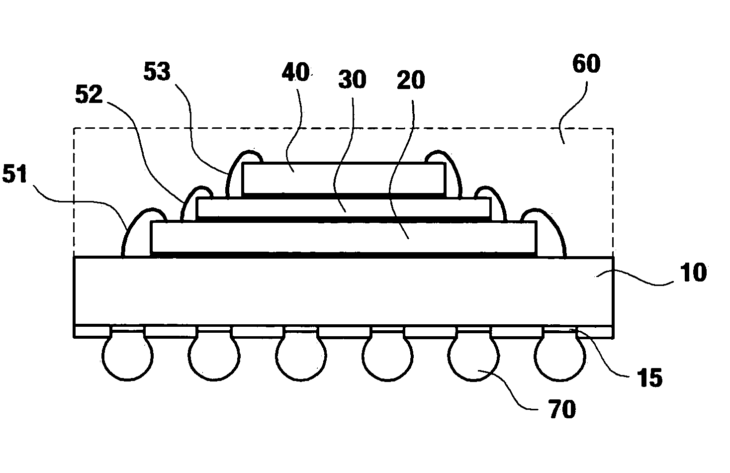
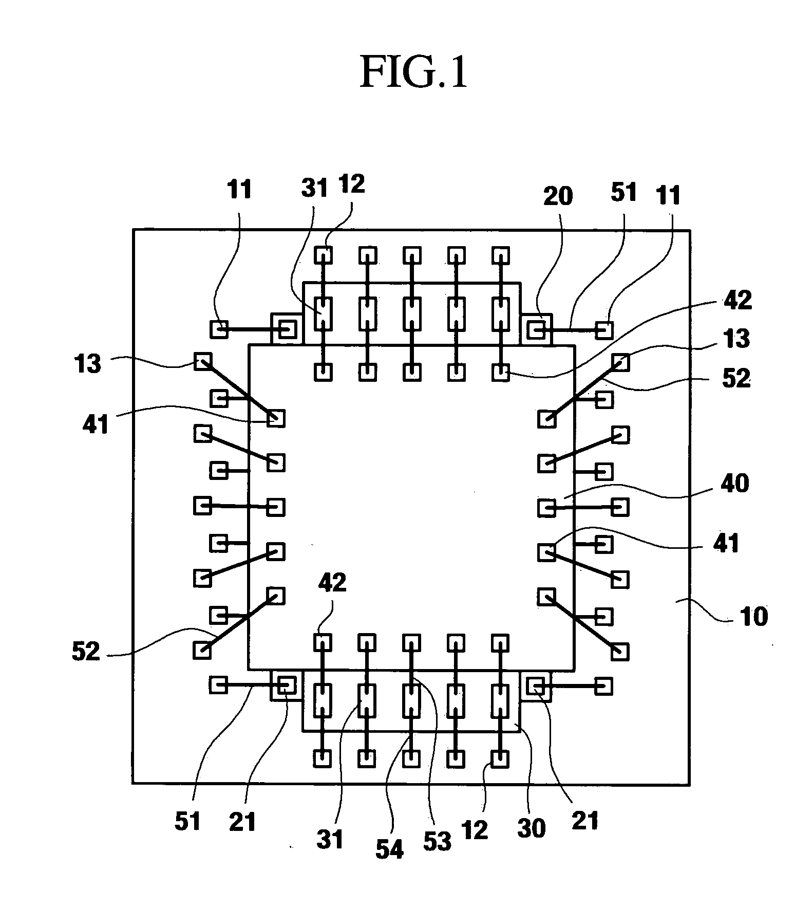
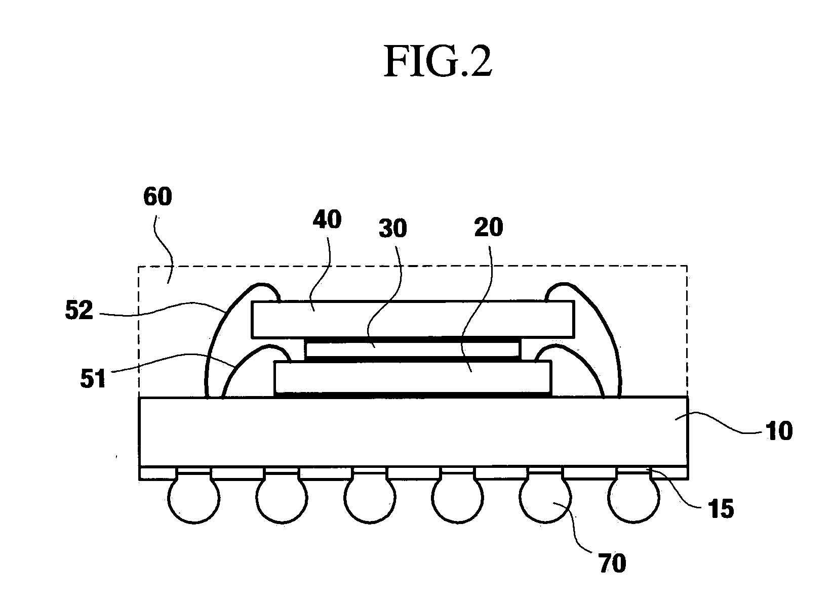
[0035] Advantages and features of the present invention and methods of accomplishing the same may be understood more readily by reference to the following detailed description of exemplary embodiments and the accompanying drawings. The present invention may be embodied in different forms and should not be construed as being limited to the embodiments set forth herein. These exemplary embodiments are provided such that this disclosure will be thorough and complete and will fully convey the concept of the invention to those skilled in the art, and the present invention will only be defined by the appended claims. Like reference numerals refer to like elements throughout the specification.

[0036] In particular, the relative thicknesses and positioning of layers or regions may be reduced or exaggerated for clarity. Further, a layer is considered as being formed “on” another layer or a substrate when formed either directly on the referenced layer or the substrate or formed on other layer...


PUM


Abstract

A multi-chip package may be provided which may include a substrate, on which multiple substrate bonding pads may be formed and under which multiple terminals may be formed, first and second semiconductor chips, which may be deposited on the substrate, and a spacer, which may be formed between the first and second semiconductor chips to have at least power and ground pads. The spacer may be used as passive element, and the first and second semiconductor chips and the power and ground pads of the spacer may be electrically connected. The pads of the semiconductor chip which may be deposited on the spacer may also be electrically connected to substrate bonding pads via the pads which may be formed on the spacer.

Description

CROSS-REFERENCE TO RELATED APPLICATIONS [0001] This application claims priority of Korean Patent Application No. 10-2004-0002373 filed on Jan. 13, 2004 in the Korean Intellectual Property Office, the disclosure of which is incorporated herein by reference in its entirety. [0002] 1. Field of the Invention [0003] The present invention relates to a multi-chip package, more particularly, to a multi-chip package in which multiple chips may be vertically stacked with spacers interposed between each of the chips and the spacers may serve as passive elements. [0004] 2. Description of the Related Art [0005] In the portable electronic equipment market, an important challenge may be packing many elements into such equipment as possible. [0006] Several ways may be used to attain thinner, smaller and / or lighter elements, a system-on-a-chip (SOC) technique in which multiple individual elements may be integrated into a single chip, and a system-in-package (SIP) technique in which multiple individu...

Claims


Application Information

Patent Timeline
IPC IPC(8): H01L25/07G11C11/34G11C16/02G11C16/06G11C16/10G11C16/34H01L21/44H01L21/50H01L21/52H01L21/60H01L23/00H01L23/12H01L23/34H01L23/48H01L23/488H01L23/50H01L25/00H01L25/065H01L25/18H05K3/30H05K5/00H05K5/04H05K5/06
CPCH01L2224/49433H01L2924/07802H01L2924/01004H01L2924/01005H01L2924/01006H01L2924/01014H01L2924/0102H01L2924/01033H01L2924/01079H01L2924/15311H01L2924/19041H01L2924/30107H01L2924/01002H01L2924/10253H01L2224/92247H01L2224/73265H01L2224/32225H01L2924/014H01L2224/49175H01L2224/49171H01L2224/4911H01L2224/48227H01L2224/48145H01L2224/48091H01L2224/45144B82Y10/00G11C16/10G11C16/3454G11C16/3459G11C2216/14H01L24/45H01L24/49H01L2224/32145H01L2924/00014H01L2924/00H01L2924/00012H01L2924/181H01L24/73H01L2224/05554H01L2224/48265H01L2225/0651H01L2924/19102H01L2924/19104H01L2924/19107H01L2225/06572H01L24/48H01L23/12H05K3/30H01L21/52
Inventor YOON, KI-MYUNGKWON, HEUNG-KYULEE, HEE-SEOK
Owner SAMSUNG ELECTRONICS CO LTD
Why Eureka
Try Eureka