

Light-emitting device, method of manufacturing light-emitting device, and electronic apparatus
a technology of light-emitting devices and electronic devices, which is applied in the direction of discharge tubes/lamp details, electric discharge lamps, discharge tubes luminescnet screens, etc., and can solve problems such as light-emitting failures
- Summary
- Abstract
- Description
- Claims
- Application Information
AI Technical Summary
Benefits of technology
Problems solved by technology
Method used
Image

Examples
first embodiment
[0057] (Light-Emitting Device)
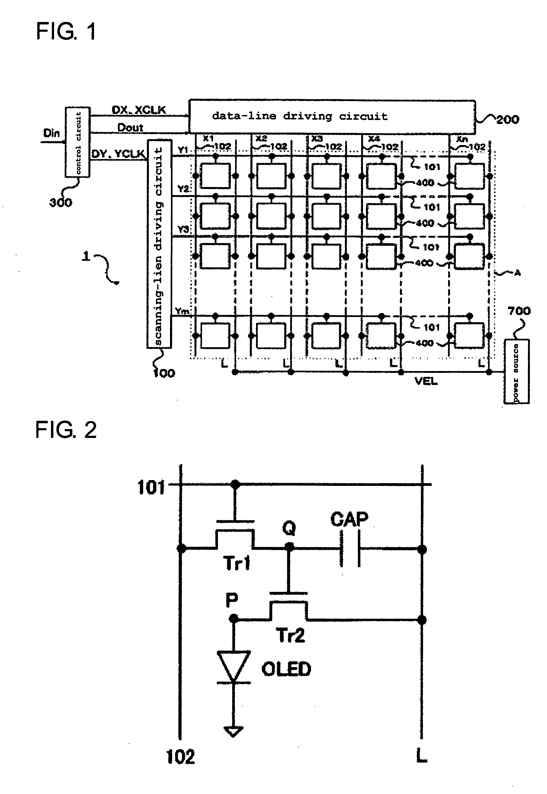
[0058]FIG. 1 is a block diagram schematically illustrating a structure of a light-emitting device 1 according to the present invention. The light-emitting device 1 comprises a pixel area A, a scanning-line driving circuit 100, a data-line driving circuit 200, a control circuit 300, and a power source circuit 700. In the pixel area A, m scanning lines 101 are formed parallel to the X direction. n data lines 103 are formed parallel to the Y direction perpendicular to the X direction. Pixel circuits 400 are provided to correspond to intersections between the scanning lines 101 and the data lines 103. Each pixel circuit 400 includes a light-emitting element OLED. Each pixel circuit 400 is supplied with source potential VEL generated from the power source circuit 700 through a plurality of power source lines L. In this example, the power source lines L are provided to be parallel to the data lines 103, and the source potential VEL is supplied from one end t...
second embodiment
[0112] Next, a second embodiment of the present invention will be described. The light-emitting device according to the second embodiment is substantially equal to the light-emitting device according to the first embodiment, except for the shape of the adhesion portion and the manufacturing method thereof. Therefore, the same constituent elements are denoted by the same reference numerals and the detailed description thereof is omitted.
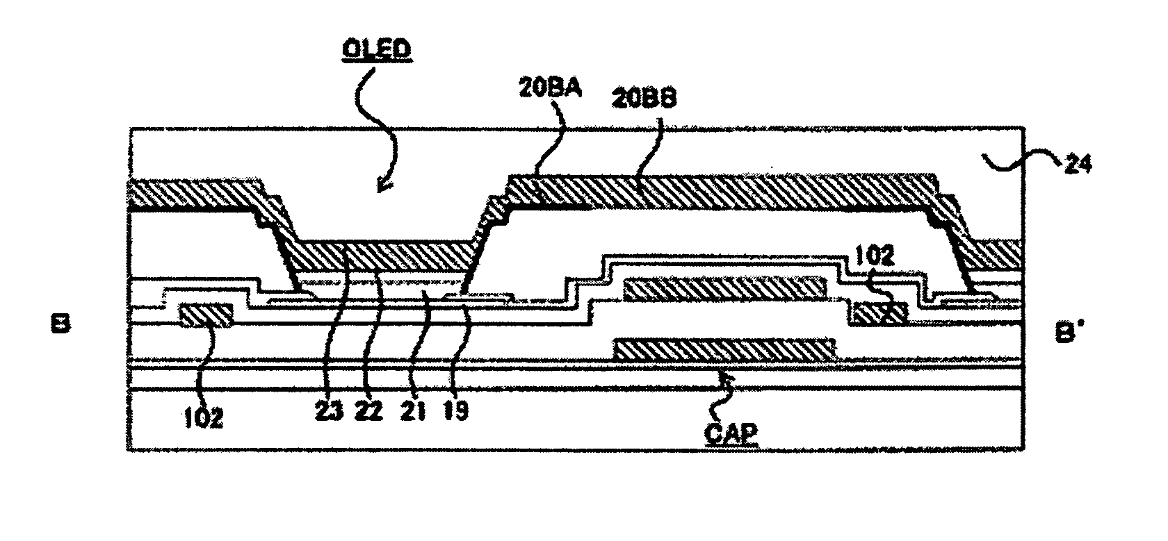
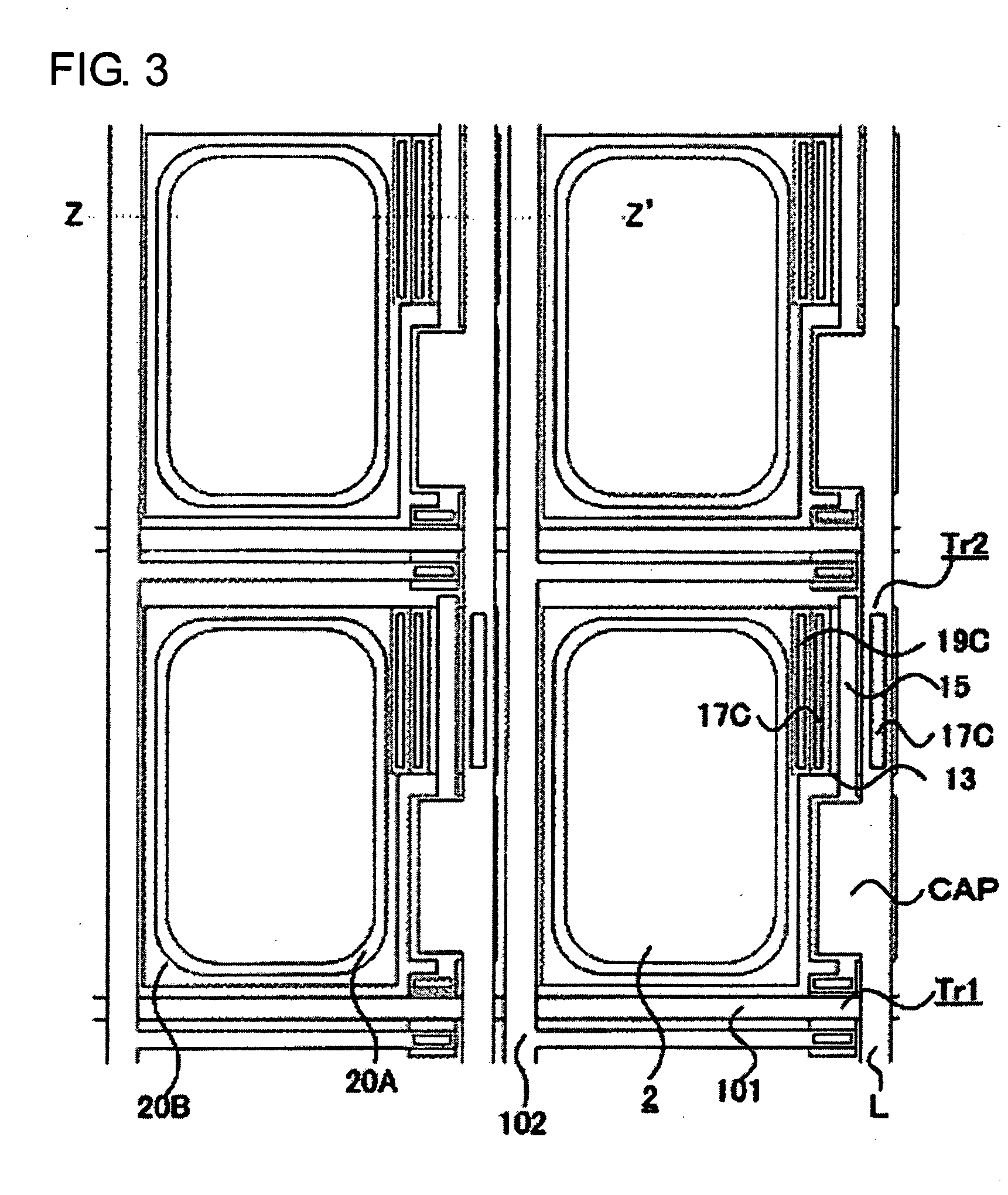
[0113]FIG. 8 is a plan view illustrating the light-emitting device according to the second embodiment, FIG. 9 is a cross-sectional view taken along Line A-A′ shown in FIG. 8, and FIG. 10 is a cross-sectional view taken along Line B-B′ shown in FIG. 8.
[0114] As shown in FIG. 8, the adhesion portions 20BB of the second partition wall portion 20B indicated by the hatched portion are provided to correspond to the storage capacitors CAP, the intersections between scanning lines 101 and the data lines 102 or the intersections between the scanning lines 10...
third embodiment
[0121] Next, a third embodiment of the present invention will be described with reference to FIG. 12. The light-emitting device according to the third embodiment is substantially equal to the light-emitting device according to the aforementioned embodiments, except for the shape of the adhesion portion and the manufacturing method thereof. Therefore, the same constituent elements are denoted by the same reference numerals and the description thereof is omitted.
[0122]FIG. 12 is cross-sectional views illustrating a method of manufacturing an organic EL device according to the third embodiment.
[0123] First, as shown in FIG. 12E, the second partition wall portion 20B is formed on the first partition wall portion 20A. Next, as shown in FIG. 12F, a known photoresist M is formed in at least a part of the top area A0 of the top wall portion on the second partition wall portion 20B and in the pixel forming area 2 indicated by an area A2, other than the area A1 of the second partition wall ...
PUM
 Abstract
Description
Claims
Application Information