Laser trim motion, calibration, imaging, and fixturing techniques

a laser beam and motion technology, applied in the field of energy beam scanning, can solve the problems of /b> being typically in a distorted pattern, laser beam and camera not coaxial, pin cushion-type field pattern, etc., and achieve the effect of optimizing lasing procedures

Inactive Publication Date: 2005-09-22
THE GSI GRP LLC
View PDF14 Cites 139 Cited by
  • Summary
  • Abstract
  • Description
  • Claims
  • Application Information

AI Technical Summary

Benefits of technology

[0030] Another embodiment of the present invention provides a system for probing circuit elements. The system includes a fixture having a surface configured to support a work piece having a target element. The fixture includes a calibration subassembly configured to aid automatic calibration during at least one of probe card planarization, probe card alignment, galvo calibration, laser power measurement, and probe tip cleaning. A probe holder is configured to support a probe for detecting a characteristic of the target element. A first stage is configured to rotate the probe holder about an axis substantially orthogonal to the surface, so as to automatically align probe tips of the probe with corresponding probe locations associated with the target element (e.g., O-direction stage). In one such embodiment, the calibration subassembly is accessible even when work piece is mounted on the fixture, thereby allowing real-time automatic calibration procedures to be carried out.
[0031] Another embodiment of the present invention provides a system for positioning a work piece for lasing. The system includes a fixture having a surface substantially parallel to a plane and defined by a first axis and a second axis that is orthogonal to the first axis, the surface for supporting a work piece configured with a plurality of different areas disposed thereon, with each area including one or more circuit elements to be lased. A first stage is configured to move the fixture substantially parallel to the plane and the first axis, and a second stage is configured to move the first stage and the fixture substantially parallel to the plane and the second axis. A controller is configured to determine a path for movement between the different areas by directing movement of the first stage and the second stage based on distances along the first axis between each of the different areas and distances along the second axis between each of the different areas, thereby positioning each of the plurality of different areas for lasing the one or more circuit elements included in that area. The controller can be configured, for example, to determine a path for movement that is associated with a travel time that is comparable or shorter than travel time of other possible paths. Thus, optimal lasing procedures can be achieved.

Problems solved by technology

Such distortions will otherwise result in a pin cushion-type of field pattern.
However, the marks 220 are typically in a distorted pattern naturally because of the distortions and non-linearity inherent to the system.
In conventional laser-trimming systems with through-the-lens camera viewing via the beam-directing device, one problem is that the laser beam and cameras typically are not coaxial.
A major problem with both of these calibration options is that a sacrificial plate 210 or reference grid 300 must be placed into the machine prior to this operation.
This requires operator intervention and thus cannot be done in an automated fashion during processing.
Another problem associated with conventional laser trimming systems is that there is a requirement to maintain parallelism of the probe tips relative to the work piece that is being probed during trimming.
Additionally, for very fine pitch applications, such as applications requiring the probing of elements on a work piece, it is not possible to visually determine the position of the probe tips since the adjustments are so small.
Thus, the planarization alignment process is cumbersome in that it is manual, iterative, and requires significant operator intervention.
Further, the accuracy of the results is marginal.
A major problem with these techniques is that the process is manual and iterative and vision subsystems are often not able to see the correct location of the probe tip because they are unable to focus on a probe that is not perfectly planar with the substrate.
Thus, conventional techniques for aligning probe card tips with the circuit probe pads require substantial time and operator effort in order to achieve proper alignment.
One of the major problems with conventional substrate alignment techniques is that the edges of the printed circuit board (PCB) panel are typically not well defined with reference to the circuits within the edges.
Therefore, aligning the panel to edge stops will not greatly improve the alignment of the circuits formed on the panel.
A second problem is that the circuits or any underlying components on the underside of the panel are prone to damage if the panel is translated when in contact with the substrate fixture.
A third problem is the mechanical difficulty encountered when rotating larger panels mounted on top of an X-Y stage.
All of these issues are further exacerbated by large panel sizes typically used in PCB production, which implicates larger substrate fixtures.
This results in down-time and / or operator intervention, and hence lowers the efficiency of the machine processing.
The panel fixture is typically fairly large and heavy for large PCB panels, and this weight means that the speed (velocity and acceleration), of the X-Y stage in moving such panels is typically quite slow.
Furthermore, the larger travel distance required to cover these large PCB panels causes the accuracy of the X-Y stage 810 movement to degrade as the required movement distance increases.
As the stage moves further and further away from that location, there is an accumulation of errors that results in the lowering of the accuracy of movement.
The time for this step and repeat motion between the trimming / probing locations is overhead that adds to the total process time for the substrate.
However, for large PCB panels, especially where the number of individual probing and trimming sites on the panel is also large, this step and repeat overhead time can become a significant fraction of the total process time.
Furthermore, the large size of the PCB panels to be trimmed typically infers a larger and higher mass of the substrate fixture, the movement of which will be at a slower acceleration and velocity than the acceleration and velocity at which a smaller substrate fixture used for convention small substrates can be moved.

Method used


Image

  • Laser trim motion, calibration, imaging, and fixturing techniques
  • Laser trim motion, calibration, imaging, and fixturing techniques
  • Laser trim motion, calibration, imaging, and fixturing techniques

Examples


Embodiment Construction

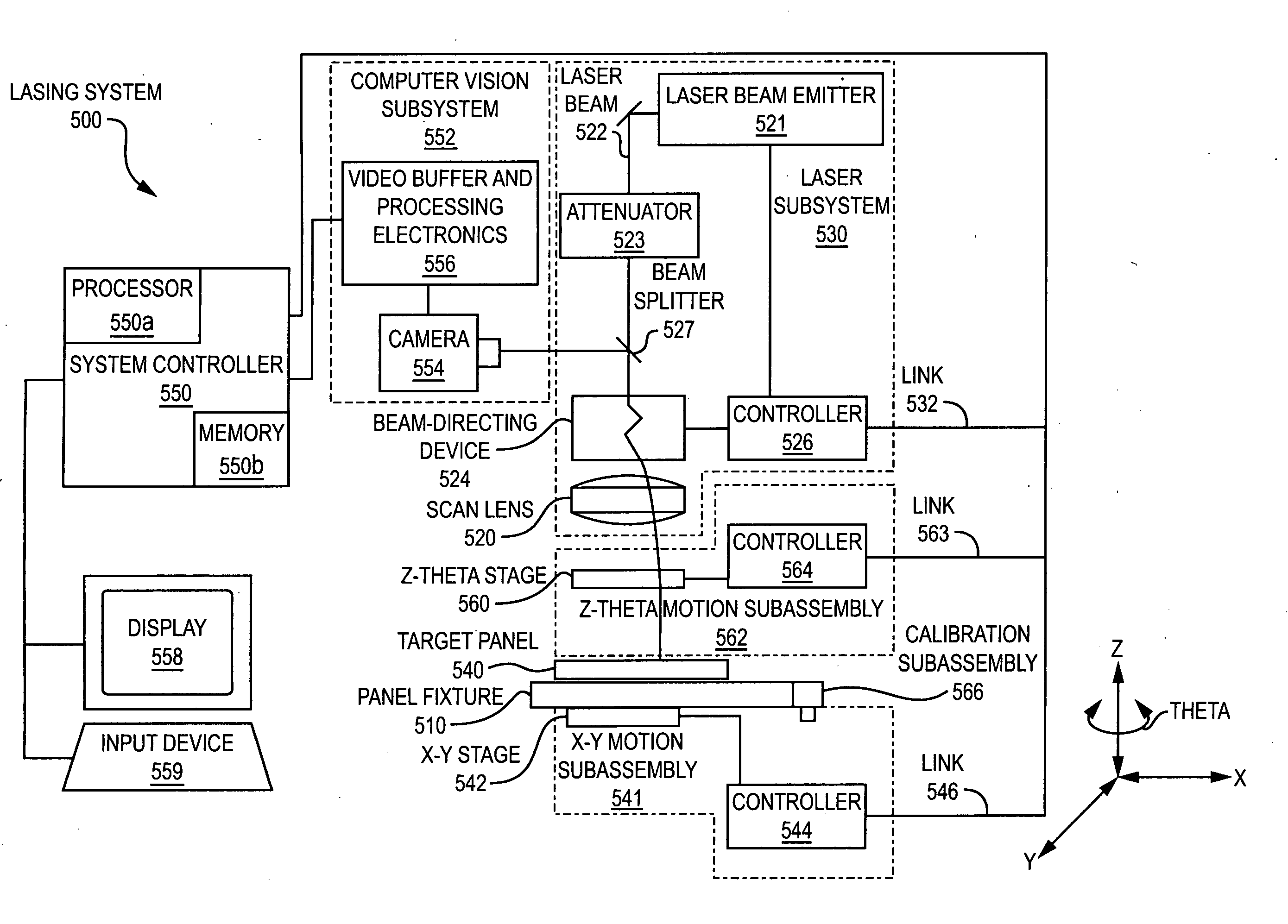
[0078] Embodiments of the present invention enable calibration of a vision subsystem and / or a laser beam in a lasing system without the use of a sacrificial plate or a reference grid or plate, and without operator intervention and in a substantially automated fashion. Planarization of the probe card and the surface of the work piece is enabled with a high degree of accuracy, and in a less cumbersome manner relative to conventional techniques. Proper alignment of probe card tips with circuit probe pads can be achieved more quickly and more easily. Likewise, accurate alignment of circuits or circuit elements on a panel or other substrate without damage to circuits or elements on the underside of the substrate and / or without the need to rotate the substrate is enabled. Also, efficient lasing of different circuits laid out on a single substrate with different orientations is enabled. In a more general sense, the disclosed techniques can be employed to reduce overall lasing time for proc...


PUM

PropertyMeasurementUnit
angleaaaaaaaaaa
diameteraaaaaaaaaa
wavelengthaaaaaaaaaa

Abstract

A system for probing circuit elements, includes a panel fixture, probe holder and stage. The fixture has a platen surface to support a work piece having work piece surface. The work piece surface is substantially parallel to the platen surface and has a target element thereon. The probe holder is configured to support a probe for detecting a characteristic of the target element. A stage rotates the probe holder about an axis substantially orthogonal to the platen surface, to align the probe with probe locations associated with the circuit element, so that the characteristic of the circuit element can detected by the probe. Fixturing motion can be optimized for efficient work piece manufacturing. Calibration and vision subassemblies are also provided.

Description

RELATED APPLICATIONS [0001] This application claims the benefit of U.S. Provisional Application No. 60 / 512,048, filed Oct. 17, 2003, which is herein incorporated in its entirety by reference.FIELD OF THE INVENTION [0002] The invention relates to energy beam scanning, and more particularly, to laser trim motion, calibration, imaging, and fixturing techniques. BACKGROUND OF THE INVENTION [0003] It is known to change the electrical properties of passive and some active electronic elements by removing material therefrom. Methods of removing material include applying laser energy for vaporizing a portion of the material, applying laser energy for ablative removal of the material, and applying laser energy to affect a photochemical reaction for removing and / or otherwise altering an electrical performance characteristic of the material. The relative effect of these three processes depends on the energy density and wavelength of the laser, and the properties of the material illuminated by t...

Claims


Application Information

Patent Timeline
Patent Type & Authority Applications(United States)
IPC IPC(8): B23K26/00B23K26/03B23K26/08B23K26/36B23K26/38B23K26/40G21K7/00H05K1/02H05K3/00
CPCB23K26/0003B23K26/4005B23K26/0853B23K26/367B23K26/381B23K26/4075B23K2201/42H05K1/0269H05K3/0008H05K3/0026H05K3/0097H05K2201/09918B23K26/0807B23K26/426B23K26/041B23K26/032B23K26/351B23K26/082B23K26/042B23K26/364B23K26/705B23K26/382B23K26/40B23K2101/42B23K2103/50
Inventor KITAI, ANTON T.MANK, ANDREASLABELLE, PAUL A.NAUMOV, ANDREIMILLER, IAN J.PARKER, ROBERT G.
Owner THE GSI GRP LLC
Why Eureka
Try Eureka