Supercharge Your Innovation With Domain-Expert AI Agents!

ESD protection device with high voltage and negative voltage tolerance

Active Publication Date: 2005-09-22
ORISE TECHNOLOGY CO LTD
View PDF2 Cites 15 Cited by
  • Summary
  • Abstract
  • Description
  • Claims
  • Application Information

AI Technical Summary

Benefits of technology

[0009] Another object of the present invention is to provide an ESD protection device with positive voltage and negative voltage tolerance, and the ESD protection device can quickly bypass the electrostatic discharge pulse out of the protected circuit.
[0013] The present invention uses the floating first type wells (e.g., the P-type well), the isolation structure (e.g., the field oxide region) and the transistor structure (e.g., the NPN transistor) that is turned on during an electrostatic discharge, to provide ESD protection. Because the first type well is floating, when an electrostatic pulse occurs, the PN junction in the ESD protection device breaks down and hence, a transient current is generated. The transient current turns on the transistors in the ESD protection device (including the lateral transistor and the vertical transistor). Hence, the ESD protection device of the present invention introduces the electrostatic pulse to the system voltage line or the ground line so as to prevent the internal circuit from damage caused due to ESD.

Problems solved by technology

Electronic components and circuits, which are not provided with suitable protection, are highly susceptible to ESD damage.
Since ESD voltage is much larger than the power supply voltage, ESD voltage will damage adjacent semiconductor devices when the ESD phenomenon occurs.
For the traditional ESD protection devices, it is impossible to offer ESD protection for positive and negative voltages by a single ESD protection device.

Method used


Image

  • ESD protection device with high voltage and negative voltage tolerance
  • ESD protection device with high voltage and negative voltage tolerance
  • ESD protection device with high voltage and negative voltage tolerance

Examples


Embodiment Construction

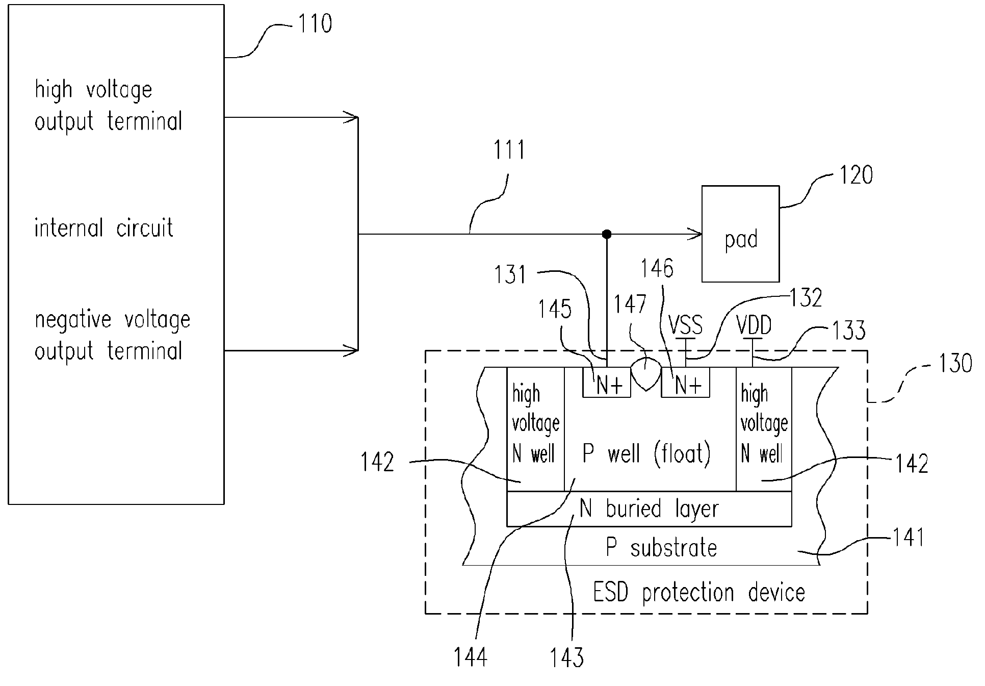
[0018] A large number of ICs output (or input) positive and negative voltage signals in a single connecting terminal. For example, a source driver IC of a LCD panel is required to output positive voltage as well as negative voltage signals in a single connecting terminal (the channel for driving the LCD panel). Hence, according to one embodiment of the present invention, an ESD protection device having positive voltage and negative voltage tolerance is provided for ESD protection.

[0019]FIG. 1 illustrates the circuit diagram of an ESD protection device providing both positive and negative voltage protection, in accordance with one embodiment of the present invention. Within the IC package, an internal circuit 110 is the circuit being protected by an ESD protection device 130. Pad (bonding pad) 120 is a coupling element that connects internal circuit 110 to the lead of the IC package. Internal circuit 110 outputs both a high (positive) voltage signal and a negative voltage signal via...


PUM


Abstract

An electrostatic discharge protection device with high voltage and negative voltage tolerance is provided. The electrostatic discharge protection device comprises: a first type substrate; a first type well inside the first type substrate, the first type well being floating; a second type well inside the first type substrate, the second type well separating the first type well from the first type substrate, the second type well being coupled to a first voltage line; a second type first doped region inside the first type well and coupled to a second voltage line; a second type second doped region inside the first type well and coupled to the pad; and an isolation structure between the second type first doped region and the second type second doped region.

Description

CROSS-REFERENCE TO RELATED APPLICATION [0001] This application claims the priority benefit of Taiwan application serial no. 93107620, filed on Mar. 22, 2004. BACKGROUND OF THE INVENTION [0002] 1. Field of the Invention [0003] The present invention relates to an electrostatic discharge (ESD) protection device. More specifically, the present invention relates to an ESD protection device with both positive voltage and negative voltage tolerance. [0004] 2. Description of Related Art [0005] ESD damage is usually caused by direct electrostatic discharge from a charged conductor to an electrostatic discharge sensitive device (ESDS), electrostatic discharge from the ESDS or by field-induced discharges. ESD simulation models include the human-body model (HBM), the machine model (MM), and the charge-device model (CDM). Electronic components and circuits, which are not provided with suitable protection, are highly susceptible to ESD damage. [0006] Since the electronic products are required to ...

Claims


Application Information

Patent Timeline
IPC IPC(8): H01L23/60H01L23/62H01L27/02
CPCH01L27/0259
Inventor WANG, TAI-HO
Owner ORISE TECHNOLOGY CO LTD
Features
  • R&D
  • Intellectual Property
  • Life Sciences
  • Materials
  • Tech Scout
  • Unparalleled Data Quality
  • Higher Quality Content
  • 60% Fewer Hallucinations
Learn More