Method for forming an ESD protection circuit

a protection circuit and rectifier technology, applied in the field of electrostatic discharge protection circuits, can solve the problems of affecting the performance of the device, requiring scr to be triggered, and reducing the voltage at which damage may occur

Inactive Publication Date: 2007-10-23
CHARTERED SEMICONDUCTOR MANUFACTURING +1
View PDF9 Cites 31 Cited by
  • Summary
  • Abstract
  • Description
  • Claims
  • Application Information

AI Technical Summary

Benefits of technology

[0024]To accomplish at least one of these objects, an ESD protection circuit is formed at the input / output interface contact of an integrated circuit to protect the integrated circuit from damage caused by an ESD event. The ESD protection circuit has a polysilicon bounded SCR and a biasing circuit. The polysilicon bounded SCR is connected between a signal input / output interface contact of the integrated circuit and a power supply connection of the integrated circuit. The biasing circuit is connected to the polysilicon bounded SCR to bias the polysilicon bounded SCR to turn on more rapidly during the ESD event.
[0034]The heavily doped polycrystalline layer of the polysilicon bounded SCR and the polysilicon bounded diode permits a series resistance of the polysilicon bounded SCR and the polysilicon bound diode to be smaller for a more efficient operation. The heavily doped polycrystalline layer is connected to bias the heavily doped polysilicon layer such that salicide shorting is prevented the first and second diffusion regions and preventing of accidental formation of an inversion region heavily doped polycrystalline layer.

Problems solved by technology

In ESD protection circuits, the series resistance of the active devices affects the performance of the devices.
However, as the feature sizes of integrated circuits have become smaller, the voltages at which damage may occur is becoming smaller and the SCR needs to be triggered at lower voltages that are greater than the operating voltages of the integrated circuits.

Method used


Image

  • Method for forming an ESD protection circuit
  • Method for forming an ESD protection circuit
  • Method for forming an ESD protection circuit

Examples


second embodiment

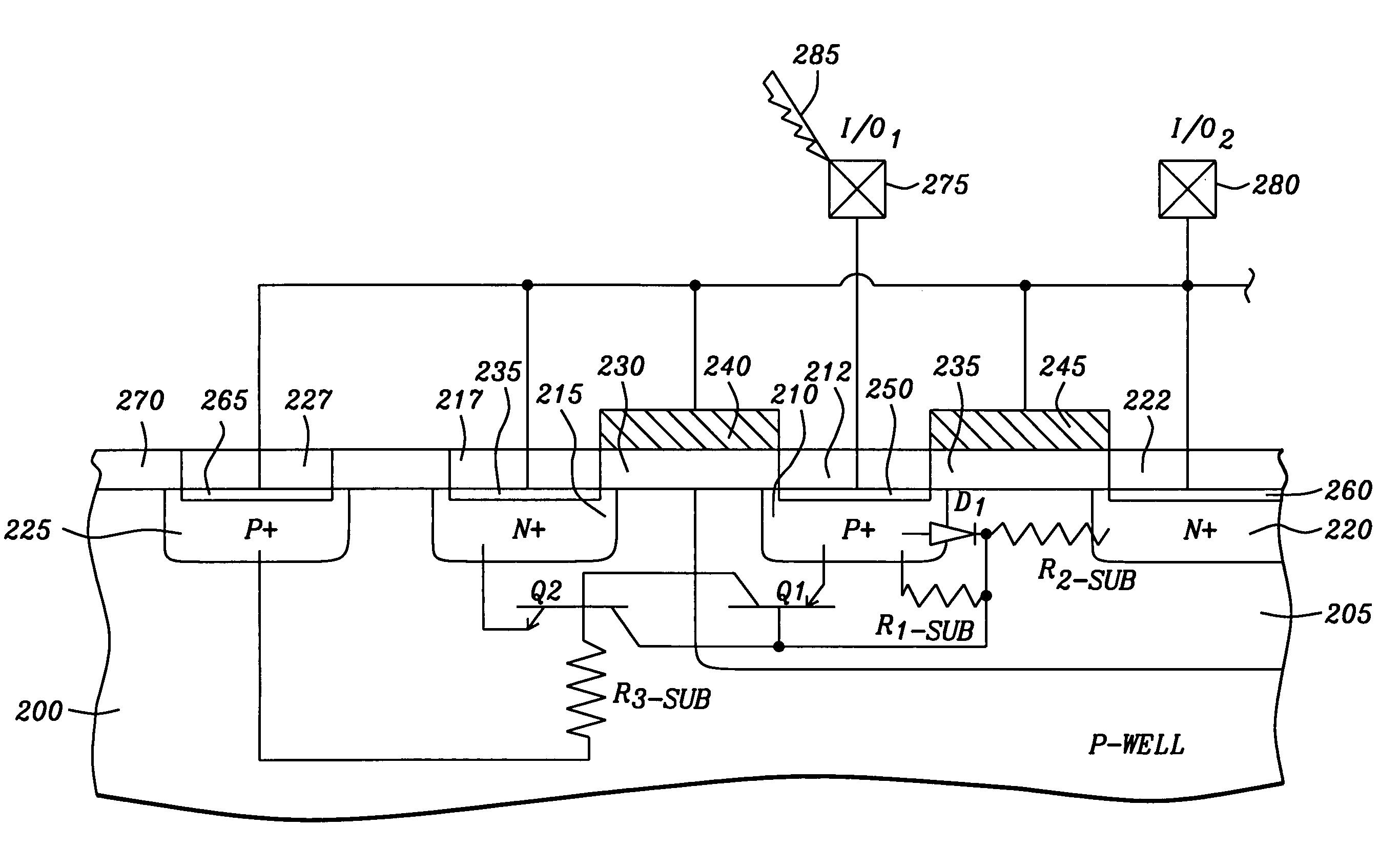
[0056]the ESD protection circuit, as shown in FIG. 6 is connected between the signal input / output interface pad 275 and the power supply connection pad 280. The SCR is formed as described in FIGS. 4a and 4b. The diodes D1 and D2 are optional diodes placed in series with the SCR between the signal input / output interface pad 275 and the SCR. These diodes are structured as the diode D1 of the FIG. 4a and increase the holding voltage of the SCR when it is turned on. The base of the transistor Q1 and the collector of the transistor Q2 is the N-well 205 of FIG. 4a and will be referred to as the first gate of the SCR. The base of the transistor Q2 and the collector of the transistor Q1 is the P-well 200 of FIG. 4a and is referred to as the second gate of the SCR. The resistor R1 is connected between the signal input / output interface pad 275 and the first gate. The capacitor C1 is connected from the first gate to the power supply connection pad 280. In this example the power supply connecti...

third embodiment

[0059]the ESD protection circuit, as shown in FIG. 7 is connected between the signal input / output interface pad 275 and the power supply connection pad 280. The SCR is formed as described in FIGS. 4a and 4b. As described above, the base of the transistor Q1 and the collector of the transistor Q2 is the N-well 205 of FIG. 4a and is referred to as the first gate of the SCR. The base of the transistor Q2 and the collector of the transistor Q1 are the P-well 200 of FIG. 4a and is referred to as the second gate of the SCR.

[0060]The diodes D1, D2, and D3 are serially connected from cathode to anode and are structured as the diode D1 of the FIG. 4a. The anode of the first diode D1 is connected to the signal input / output interface pad 275 and the cathode of the last diode D3 is connected to the second gate of the SCR. The resistor R2 is connected to the second gate of the SCR and the cathode of the last diode D3. It should be noted that while this embodiment is implemented with the three di...

fifth embodiment

[0070]the ESD protection circuit, as shown in FIG. 9 is connected between the signal input / output interface pad 275 and the power supply connection pad 280. In this embodiment, the triggering bias circuit is a resistor R and capacitor C that are formed of a first metal oxide semiconductor (MOS) transistor M1 biased to act as the resistor R and a second MOS transistor M5 connected to form the capacitor C. The MOS transistor M2 connected to bias the MOS transistor M1 to an on condition to act as the resistor R. The junction connection between the resistor R and capacitor C is connected to an input terminal of a first inverter I1 of a group of serially connected inverters I1, I2, and I3. In this embodiment the preferred implementation of the group of serially connected inverters I1, I2, and I3 is shown as three inverters however, the number of inverters maybe adjusted according to the requirements of the design.

[0071]The SCR is formed as described in FIGS. 4a and 4b. The base of the tr...


PUM

PropertyMeasurementUnit
snapback voltageaaaaaaaaaa
conductivity typeaaaaaaaaaa
conductivityaaaaaaaaaa

Abstract

An ESD protection circuit is formed at the input / output interface contact of an integrated circuit to protect the integrated circuit from damage caused by an ESD event. The ESD protection circuit has a polysilicon bounded SCR connected between a signal input / output interface contact of the integrated circuit and a power supply connection of the integrated circuit and a biasing circuit. The biasing circuit is connected to the polysilicon bounded SCR to bias the polysilicon bounded SCR to turn on more rapidly during the ESD event. The biasing circuit is formed by at least one polysilicon bounded diode and a first resistance. Other embodiments of the biasing circuit include a resistor / capacitor biasing circuit and a second diode triggering biasing circuit.

Description

BACKGROUND OF THE INVENTION[0001]1. Field of the Invention[0002]This invention relates generally to electronic circuits, and in particular to silicon controlled rectifier (SCR) structures for electrostatic discharge protection (ESD). More particularly this invention relates to polycrystalline silicon (polysilicon) bounded SCR structures and to electronic protection circuits employing polycrystalline silicon bounded SCR's.[0003]2. Description of Related Art[0004]In ESD protection circuits, the series resistance of the active devices affects the performance of the devices. Higher resistance at the voltage levels of an ESD event may lead to a voltage drop across the active devices that may destroy the device. FIG. 1 shows an ESD protection diode structure of the prior art. In this example, shallow trenches are etched within the region that will become the N-well 10 and filled with an insulating material to form the shallow trench isolation (STI) 15 are formed on the substrate. A semico...

Claims


Application Information

Patent Timeline
Patent Type & Authority Patents(United States)
IPC IPC(8): H01L21/8234H01L21/331H01L27/02H01L29/74
CPCH01L27/0262H01L29/7436Y10T29/49117H01L2924/0002H01L2924/00
Inventor MANNA, INDRAJITFOO, LO KENGYA, TAN PEEFILIPPI, RAYMOND
Owner CHARTERED SEMICONDUCTOR MANUFACTURING
Why Eureka
Try Eureka