Barrier for copper integrated circuits

a technology of integrated circuits and barriers, which is applied in the direction of semiconductor devices, semiconductor/solid-state device details, electrical apparatus, etc., can solve the problems of increasing the overall resistance of metal lines, limiting the performance of integrated circuits, and resisting metal lines as important limitations

Inactive Publication Date: 2005-09-22
TEXAS INSTR INC
View PDF2 Cites 24 Cited by
  • Summary
  • Abstract
  • Description
  • Claims
  • Application Information

AI Technical Summary

Problems solved by technology

As the operating frequency of the integrated circuit increases, the resistance of the metal lines becomes an important limitation in the performance of the integrated circuit.
This will have the negative effect of increasing the overall resistance of the metals lines.

Method used


Image

  • Barrier for copper integrated circuits
  • Barrier for copper integrated circuits
  • Barrier for copper integrated circuits

Examples


Embodiment Construction

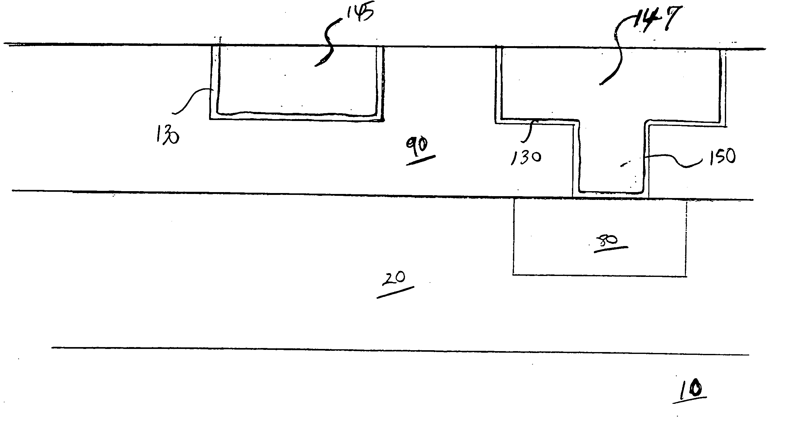
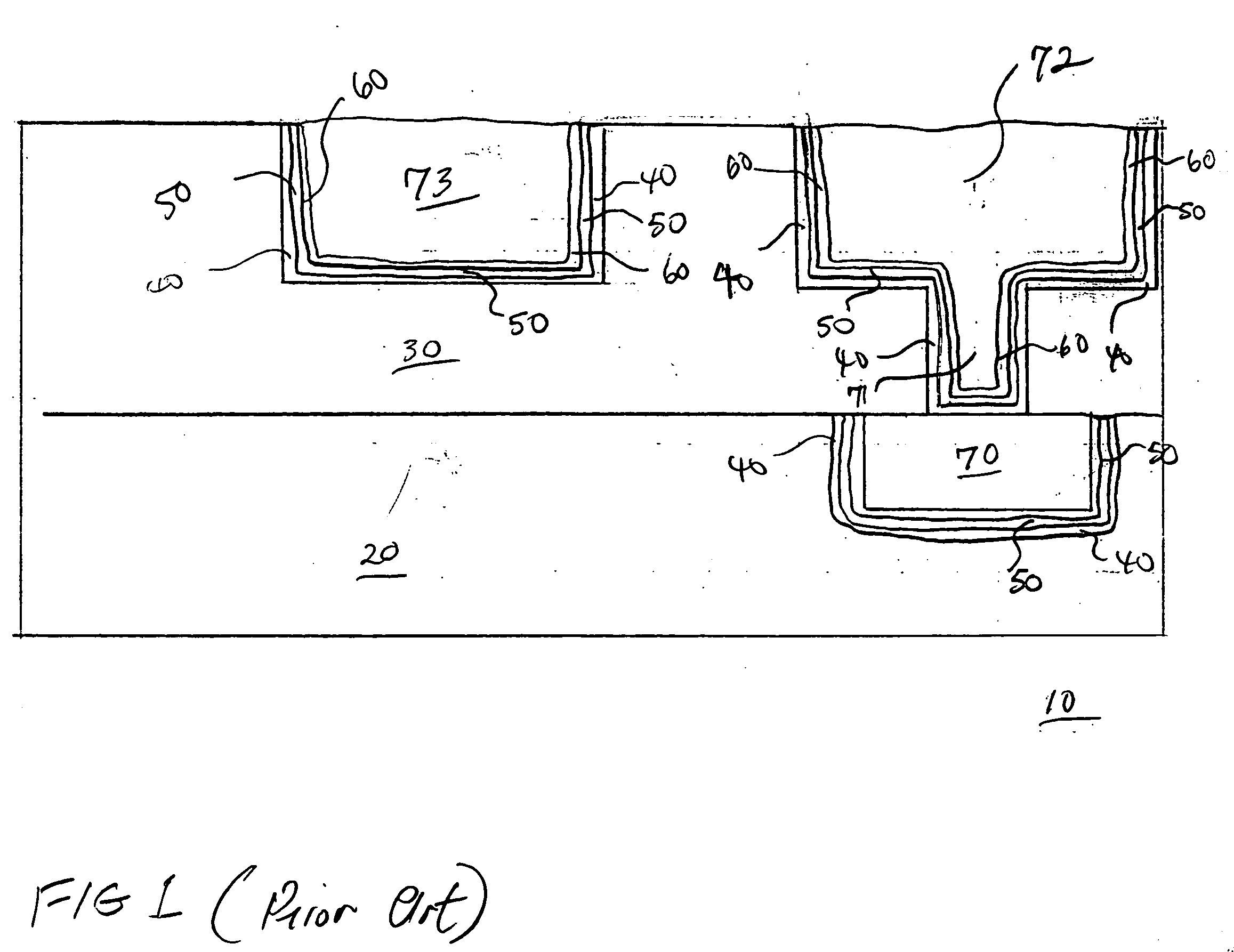
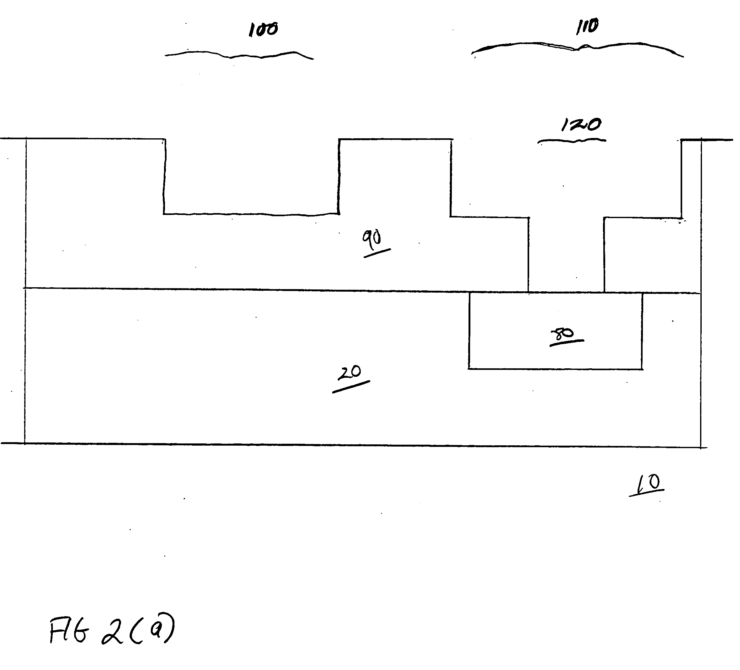
[0012] While the following description of the instant invention revolves around FIGS. 2(a) to FIG. 2(c), the instant invention can be utilized in any semiconductor device structure. The methodology of the instant invention provides a solution to reducing the size of the metal interconnect structures while significantly decreasing the overall resistivity of the lines.

[0013] The following description of the instant invention will be related to FIGS. 2(a) to FIG. 2(c). As shown in FIG. 2(a), a dielectric layer 20 is formed over a semiconductor substrate 10. The semiconductor substrate comprises electronic devices such as transistors, capacitors, diodes, etc which are not shown in the Figures for clarity. Any number of intervening layers can be formed above the semiconductor 10 and below the dielectric layer 20. The dielectric layer 20 can be formed using any suitable dielectric material. In various embodiments of the instant invention the dielectric layer 20 can comprise silicon oxide...


PUM


Abstract

An integrated circuit copper interconnect structure is formed by forming a dielectric layer (90) over a semiconductor substrate (10). Trenches (110) and vias (120) are formed in the dielectric layer (90) and a barrier layer (130) is formed in the trenches (110) and vias (120) using material such as iridium, iridium oxide, ruthenium, ruthenium oxide, rhodium, rhodium oxide, rhenium, rhenium oxide, platinum, platinum oxide, palladium and palladium oxide. Copper (147) is then used to fill the remaining area in the trenches (110) and vias (120).

Description

FIELD OF THE INVENTION [0001] The invention is generally related to the field of integrated circuits and more specifically to a novel process to form an improved barrier for copper integrated circuits. BACKGROUND OF THE INVENTION [0002] The individual electronic components that comprise an integrated circuit are interconnected by metal lines formed in dielectric layers that are themselves formed above the surface of the semiconductor substrate. As the operating frequency of the integrated circuit increases, the resistance of the metal lines becomes an important limitation in the performance of the integrated circuit. Earlier integrated circuits used aluminum to form the metal interconnect lines. However the use of aluminum is now being replaced by copper in an effort to reduce the electrical resistance of the metal interconnect lines. An example of copper interconnect lines according to the prior art is shown in FIG. 1. [0003] As shown in FIG. 1, a dielectric layer 20 is formed over...

Claims


Application Information

Patent Timeline
Patent Type & Authority Applications(United States)
IPC IPC(8): H01L21/285H01L21/768H01L21/8242H01L23/48H01L23/52H01L23/532H01L29/40
CPCH01L21/2855H01L21/28556H01L23/53238H01L21/76846H01L21/76873H01L21/76843H01L2924/0002H01L2924/00
Inventor AGGARWAL, SANJEEVTAYLOR, KELLY J.RAGHAVAN, SRINIVASGRUNOW, STEPHANPAPA RAO, SATYAVOLU S.
Owner TEXAS INSTR INC
Why Eureka
Try Eureka