
Powder metallurgy crucible for aluminum nitride crystal growth

a technology of crucibles and aluminum nitride, which is applied in the direction of crystal growth process, polycrystalline material growth, chemically reactive gases, etc., can solve the problems of aluminum gas escaping, maximum size, and lack of high-quality bulk nitride substrates

Inactive Publication Date: 2007-05-01
CRYSTAL
View PDF15 Cites 44 Cited by
  • Summary
  • Abstract
  • Description
  • Claims
  • Application Information

AI Technical Summary

Benefits of technology

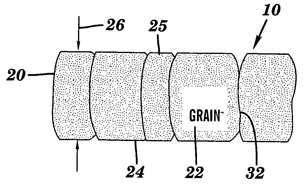
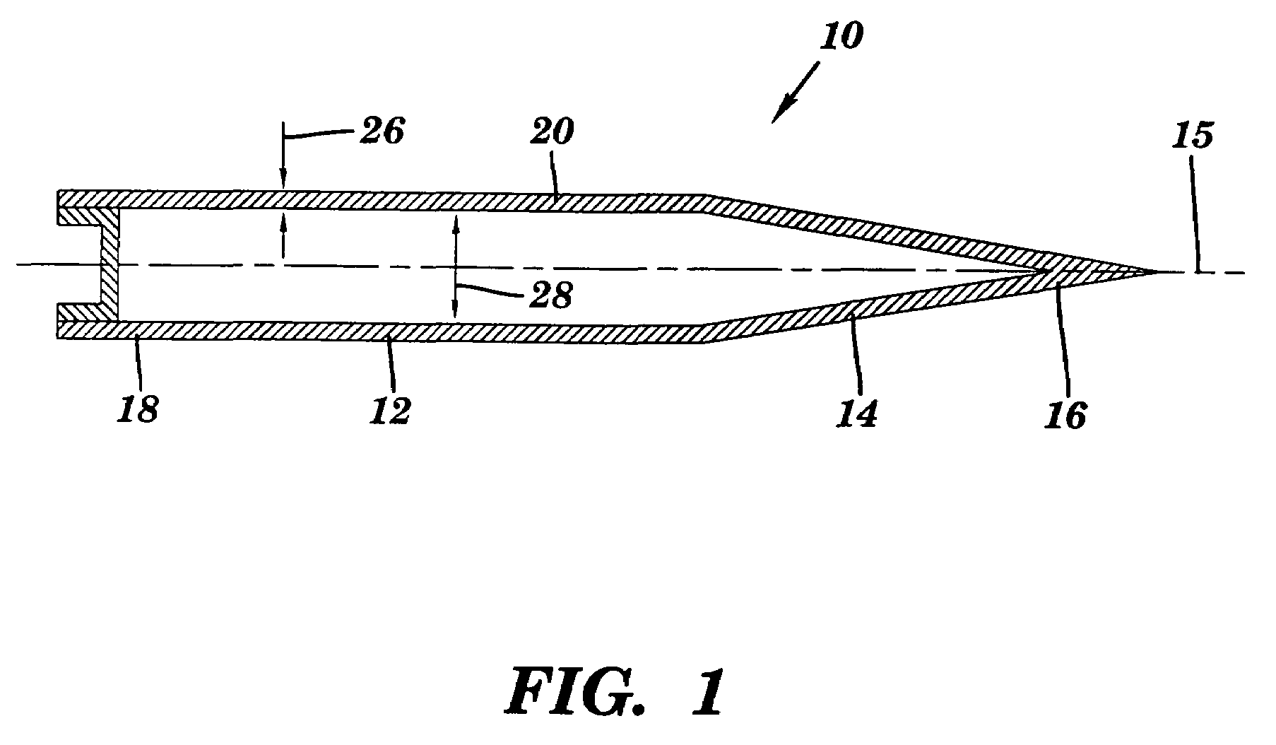
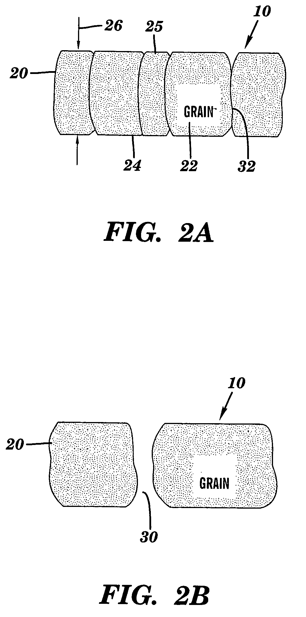
The present invention relates to a crucible for growing III-nitride semiconductor crystals. The crucible has a wall structure with a thickness dimension that is at least about 1.5 times the average grain size. The crucible also has a plurality of grains that form at least first and second layers, with the first layer including grains on the inside surface of the crucible and the second layer being adjacent to the first layer. The invention also includes a method for fabricating the crucible and a method for growing aluminum nitride single crystals using the crucible. The technical effects of the invention include improved quality and purity of the resulting crystals, as well as improved efficiency and reliability of the crystal growth process.

Problems solved by technology

However, one of the factors limiting the maturation of aluminum nitride, and other III-nitride, technology has been the absence of high-quality bulk nitride substrates.
However, one of the drawbacks that limited the maximum size of the crystals was the development of leaks in the tungsten crucibles, which ultimately lead to the failure thereof, through which aluminum gas may escape.

Method used


Image

  • Powder metallurgy crucible for aluminum nitride crystal growth
  • Powder metallurgy crucible for aluminum nitride crystal growth
  • Powder metallurgy crucible for aluminum nitride crystal growth

Examples


Embodiment Construction

[0018]Referring briefly to FIGS. 3A and 3B, the present invention includes a crucible that may be useful in growing relatively large aluminum nitride and / or other III-nitride single crystals for use in semiconductor applications. A tungsten crucible is described in this particular example. This is for illustrative purposes only and those skilled in the art will recognize the detailed description provided herein could be applied in a straightforward fashion to various other crucible materials such as described with respect to alternate embodiments described herein. The tungsten crucible 100 of this invention includes a wall structure having a thickness 126 that is at least about 1.5 times, and preferably greater than about 3 times, that of the average tungsten grain 122. In one embodiment, the tungsten crucible 100 is formed using powder metallurgy techniques.

[0019]The crucible of the present invention may advantageously provide for the growth of relatively large III-nitride single c...


PUM

PropertyMeasurementUnit
temperatureaaaaaaaaaa
pressureaaaaaaaaaa
temperatureaaaaaaaaaa

Abstract

A crucible for growing III-nitride (e.g., aluminum nitride) single crystals is provided. The crucible includes an elongated wall structure defining an interior crystal growth cavity. Embodiments include a plurality of grains and a wall thickness of at least about 1.5 times the average grain size. In particular embodiments, the crucible includes first and second layers of grains the first layer including grains forming an inside surface thereof and the second layer being superposed with the first layer. The crucible may be fabricated from tungsten-rhenium (W—Re) alloys; rhenium (Re); tantalum monocarbide (TaC); tantalum nitride (Ta2N); hafnium nitride (HfN); a mixture of tungsten and tantalum (W—Ta); tungsten (W); and combinations thereof.

Description

[0001]This application is a continuation-in-part of U.S. patent application Ser. No. 10 / 251,106 filed Sept. 20, 2002. now issued as U.S. Pat. No. 6,719,843, which claims the benefit of U.S. provisional application Ser. No. 60 / 323,947, entitled “Powder Metallurgy Tungsten Crucible for AlN Crystal Growth” filed Sep. 21, 2001. The entire disclosures of each of these applications are incorporated by reference herein.[0002]Part of the work leading to this invention was made under a United States Government STTR Contract (N00014-97-C-0362). The U.S. Government may have certain rights in this invention.BACKGROUND OF THE INVENTION[0003](1) Field of the Invention[0004]The present invention relates generally to III-nitride semiconductors and more particularly to crucibles for growing III-nitride semiconductor substrates such as aluminum nitride (AlN). Use of the crucible of this invention may enable the growth of relatively large and high quality III-nitride single crystals.[0005](2) Backgrou...

Claims


Application Information

Patent Timeline
Patent Type & Authority Patents(United States)
IPC IPC(8): C30B11/06C30B1/00C30B13/00C30B21/04C30B23/00C30B25/00C30B28/08C30B28/12C30B28/14C30B29/40C30B35/00
CPCC30B11/002C30B23/00C30B29/40C30B29/403C30B23/066C30B35/002Y10T117/1084Y10T117/108Y10T117/10
Inventor SCHOWALTER, LEO J.SLACK, GLEN A.
Owner CRYSTAL
Learn More