

Solid state imaging device
a solid-state imaging and imaging device technology, applied in the direction of radio-controlled devices, instruments, television systems, etc., can solve the problems of other chips such as the one driving the sensor circuit, the sensor circuit may malfunction, etc., and achieve the effect of preventing other chips from malfunctioning
- Summary
- Abstract
- Description
- Claims
- Application Information
AI Technical Summary
Benefits of technology
Problems solved by technology
Method used
Image

Examples
Embodiment Construction
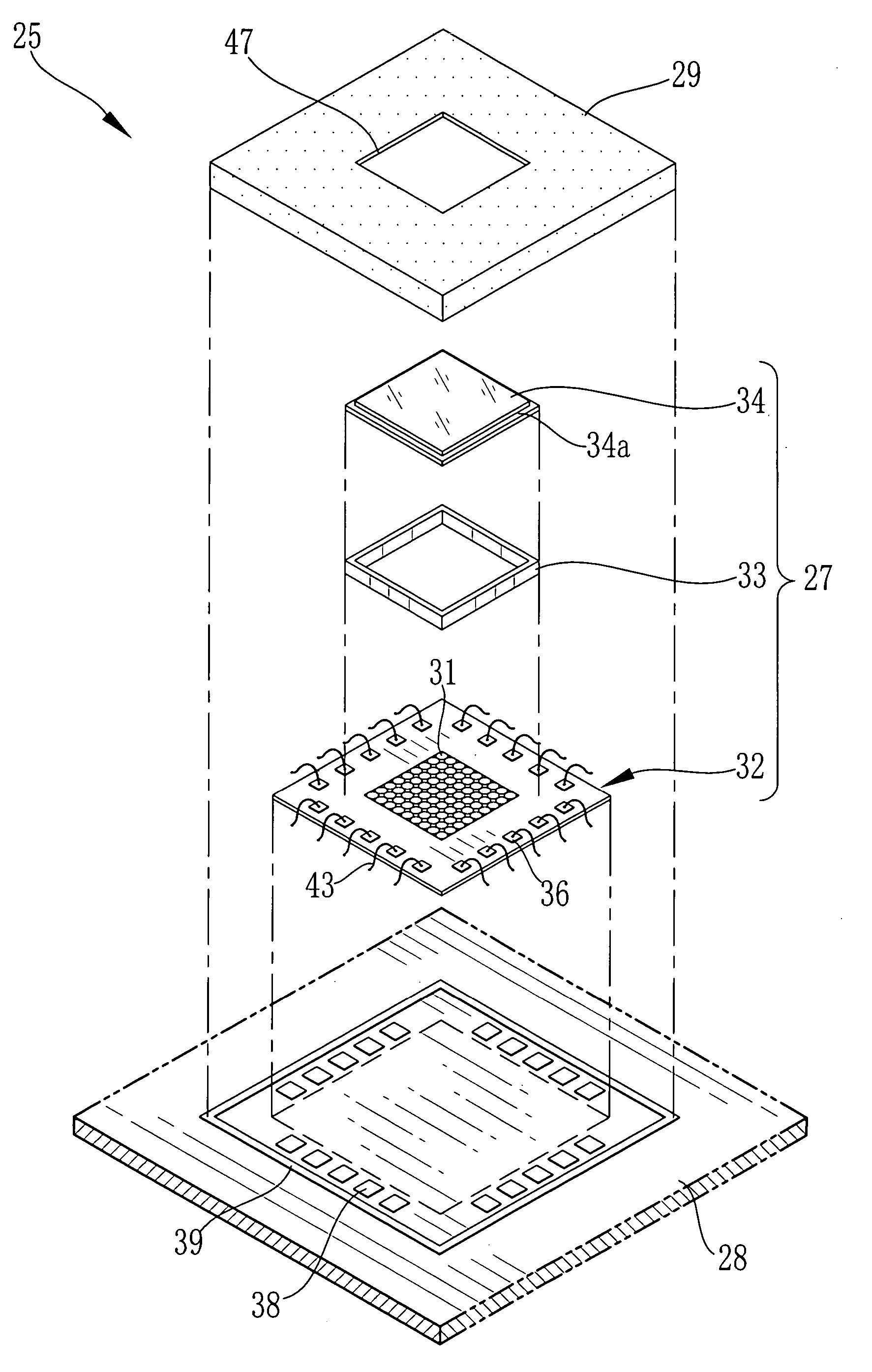
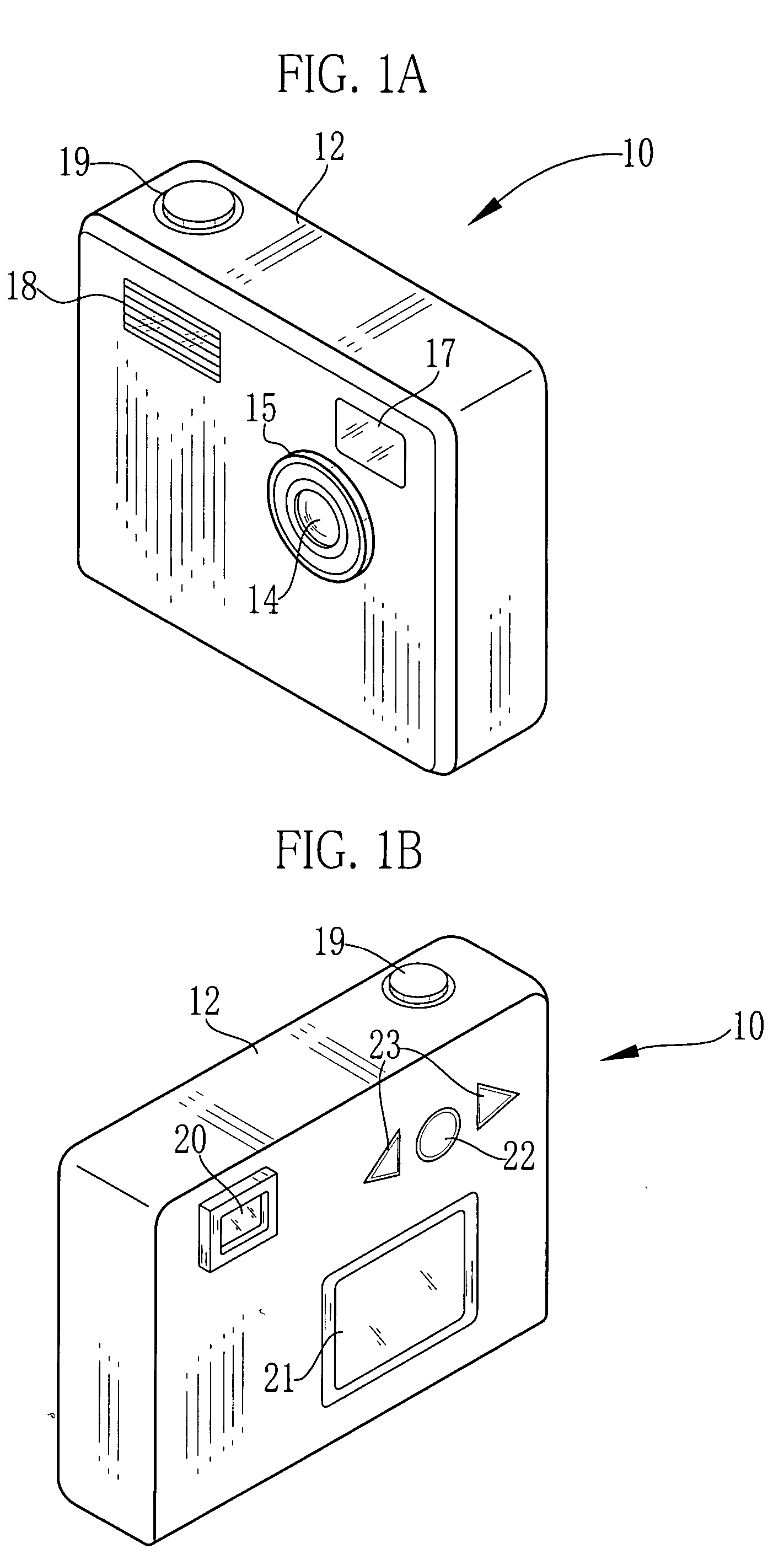
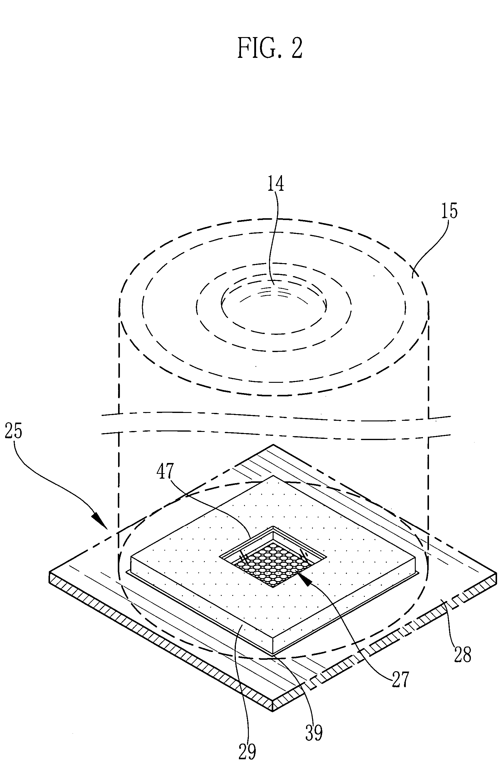
[0020] As shown in FIG. 1A and FIG. 1B, a digital camera 10 is constituted of a camera body (not shown) including photographing mechanisms and a body cover 12 which covers the camera body. On a front surface of the body cover 12, a lens barrel 15 having a taking lens 14, an object-side viewfinder window 17, a flashlight emitting unit 18 for emitting the flash light toward a subject, and so on are provided. On a top surface of the body cover 12, a release button 19 is provided.
[0021] On a rear surface of the body cover 12, an eye-side viewfinder window 20, a liquid-crystal display (LCD) 21 operable as an electric viewfinder (EVF), a mode select button 22, an operation button 23, and so on are provided. As operation modes for being selected by the mode select button, there will be a still image capturing mode for capturing still images, a moving image capturing mode for recording moving images, a play-back mode for viewing the captured still images and the recorded moving images.
[00...
PUM
 Abstract
Description
Claims
Application Information