Semiconductor package with build-up structure and method for fabricating the same

a technology of semiconductors and build-up structures, applied in the direction of semiconductor devices, semiconductor/solid-state device details, electrical apparatus, etc., can solve the problems of limited number of bond pads on the active surface, warpage of the active surface, and restriction of the total number of input/output contacts

Inactive Publication Date: 2005-09-29
SILICONWARE PRECISION IND CO LTD
View PDF15 Cites 38 Cited by
  • Summary
  • Abstract
  • Description
  • Claims
  • Application Information

AI Technical Summary

Benefits of technology

[0018] It should be noted that “rigid frame” and “rigid base” described herein are respectively referred to as a frame and a plate made of chemical engineering materials known in the art, which would not encounter warpage or deformation under a high temperature or during a temperature cycle. The medium is referred to as a material with a thermoelastic effect and low CTE, or a polymer material such as epoxy resin used for encapsulating chips in the art.

Problems solved by technology

However, the number of bond pads on the active surface is restricted by the limited area of the active surface and a pitch between adjacent bond pads.
Although the above build-up structure formed by the RDL technology may effectively increase the number of input / output contacts of the chip for electrical connection with external devices, the limited area of the active surface of the chip still sets a restriction on the total number of input / output contacts.
However, since the encapsulant 62 is not formed on a substrate with relatively greater rigidity and a central portion of the encapsulant 62 mounted with the chip 60 is thinner than a peripheral portion thereof, warpage may easily occur and cracking is produced at a position 624 due to concentrated stress during a temperature cycle in subsequent fabrication processes.
This situation would lead to a popcorn effect and further decrease the reliability of fabricated products.

Method used


Image

  • Semiconductor package with build-up structure and method for fabricating the same
  • Semiconductor package with build-up structure and method for fabricating the same
  • Semiconductor package with build-up structure and method for fabricating the same

Examples


first preferred embodiment

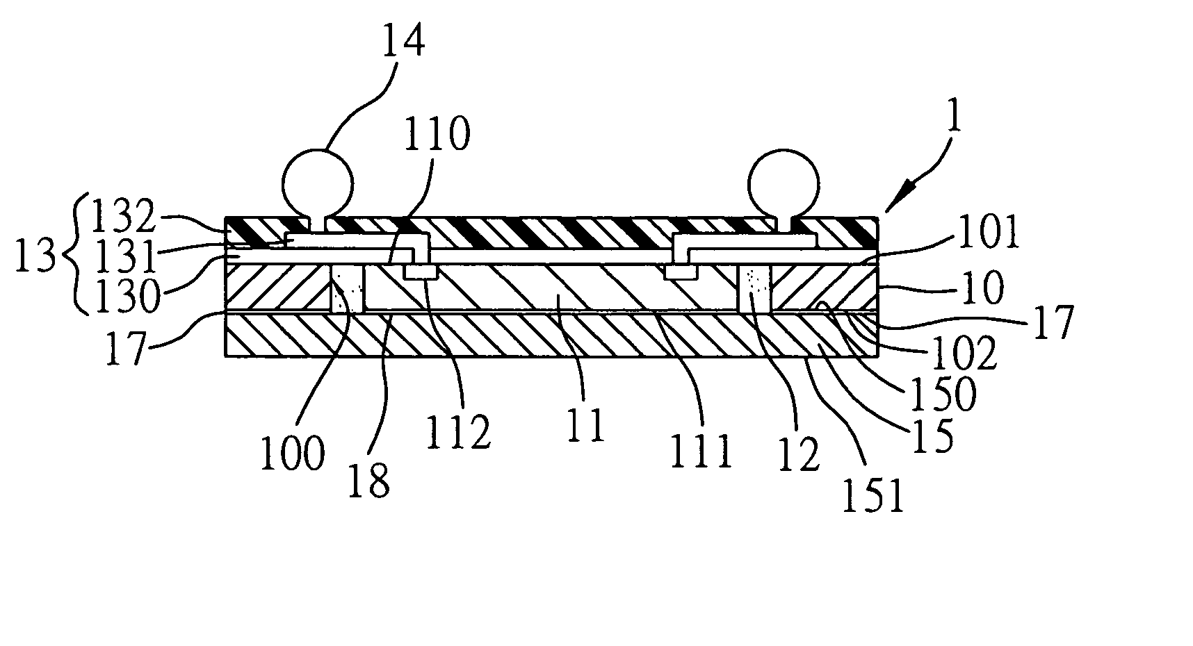
[0027] Referring to FIG. 1, a semiconductor package 1 with a build-up structure according to the present invention comprises: a rigid base 15; a rigid frame 10 with a through hole 100; a chip 11 received in the through hole 100 of the rigid frame 10; a medium such as a resin material 12 filled in a gap between the rigid frame 10 and the chip 11; a build-up structure 13 formed over the rigid frame 10 and the chip 11; and a plurality of solder balls 14 (equivalent to the foregoing conductive elements) mounted on the build-up structure 13.

[0028] The rigid base 15 and the rigid frame 10 can be made of a glass material, metal material (such as copper and the like), or thermosetting material (such as polyimide resin, bismaleimide triazine resin, FR-4 resin, and the like). The rigid base 15 and the rigid frame 10 do not encounter warpage and deformation under a high temperature or during a temperature cycle in fabrication processes and thus serve as a primary structured body of the semico...

second preferred embodiment

[0042] The method for fabricating a semiconductor package according to the second embodiment of the present invention is similar to that of the foregoing first embodiment. Therefore, only the fabrication steps in the second embodiment different from those in the first embodiment are described below with reference to FIGS. 3A to 3B. In FIGS. 3A to 3B, the same or similar components with those in FIGS. 2A to 2B are indicated by the same reference numerals.

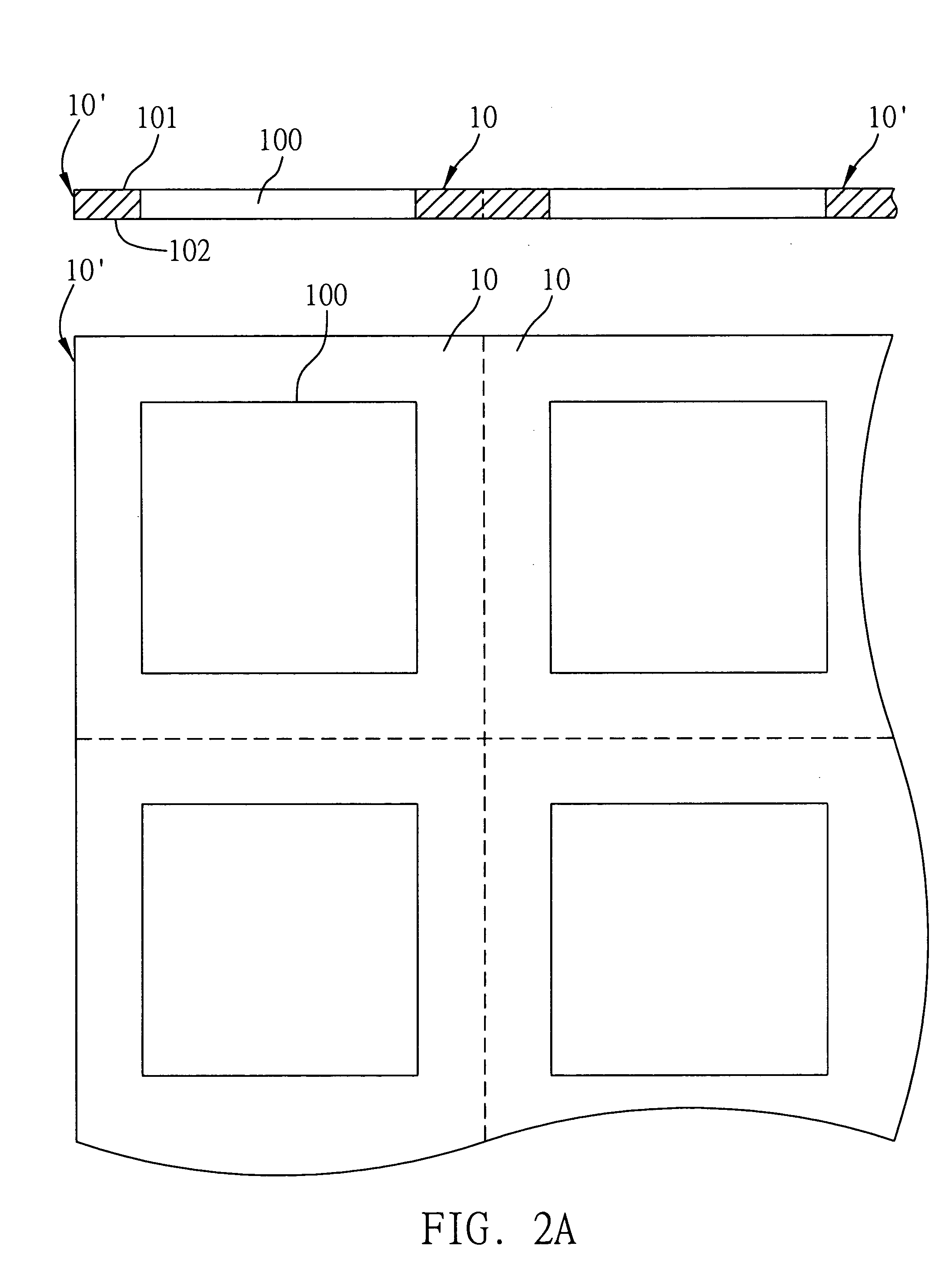
[0043] Referring to FIG. 3A, a module board 10′ comprising a plurality of rigid frames 10 arranged as an array is provided. Each of the rigid frames 10 has a rectangular through hole 100, a first surface 101, and a second surface 102 opposite to the first surface 101. Also, a rigid base 15 having a first surface 150 and a second surface 151 is provided. Moreover, a plurality of chips 11 are fixed at predetermined locations on the rigid base 15 by the following steps: applying an adhesive 18 to at least one of the first surface 150 o...

third preferred embodiment

[0047] The structure of a semiconductor package 2 disclosed in the third embodiment of the present invention is similar to that in the first embodiment, with a difference in that a rigid base 25 in the semiconductor package 2 is formed with a through hole 252 at a central position of a predetermined location thereof for mounting a chip 21 thereon as shown in FIG. 4.

[0048] The steps of fabricating the semiconductor package 2 include: preparing the rigid base 25 having a first surface 250, a second surface 251 and at least one through hole 252, wherein the through hole 252 is formed at a central position of a predetermined location on the rigid base 25 for mounting a chip; then, fixing a rigid frame 20 onto the rigid base 25 via an adhesive 27 as similarly described in the first embodiment; placing a chip 21 on the rigid base 25 and in the rigid frame 20, wherein a gap S is formed between the chip 21 and the rigid frame 20, and an inactive surface 211 of the chip 21 downwardly faces ...


PUM


Abstract

A semiconductor package with a build-up structure is provided, which includes a rigid base, a rigid frame having a through hole and fixed onto the rigid base, at least one chip received in the through hole of the rigid frame, a medium filled in a gap between the chip and the rigid frame, a build-up structure formed on the chip and the rigid frame and electrically connected to the chip, and a plurality of conductive elements bonded to the build-up structure to electrically connect the chip to external devices. The use of the rigid base and rigid frame can avoid structural warpage, cracking, delamination and a popcorn effect of the semiconductor package. A method for fabricating the semiconductor package is also provided.

Description

FIELD OF THE INVENTION [0001] The present invention relates to semiconductor packages and methods for fabricating the same, and more particularly, to a semiconductor package having a build-up structure formed on an active surface of a chip such that the distribution of external contacts where solder balls are bonded is fanned out to the area outside the active surface of the chip, and a method for fabricating the semiconductor package. BACKGROUND OF THE INVENTION [0002] Due to the requirements for compact and light-weight electronic products, semiconductor packages serving as primary components for the electronic products are being miniaturized in size. Chip Scale Package (CSP) is one kind of miniaturized semiconductor packages developed in the industry, which is characterized in that the size of such package is merely equal to or about 1.2 times larger than the size of a chip incorporated therein. [0003] In addition to the requirement for miniaturization in size, high integration a...

Claims


Application Information

Patent Timeline
Patent Type & Authority Applications(United States)
IPC IPC(8): H01L21/44H01L21/56H01L21/60H01L23/31H01L23/52H01L23/538
CPCH01L23/3128H01L24/19H01L24/97H01L2224/24226H01L2224/24227H01L2224/92H01L2224/97H01L2924/01029H01L2924/01082H01L2924/15153H01L2924/15156H01L2924/1517H01L2924/15311H01L23/5389H01L2924/01087H01L2924/01033H01L2924/01006H01L2924/01005H01L2224/83H01L2224/82H01L2924/351H01L2924/181H01L2924/12042H01L2224/73267H01L2224/12105H01L2224/04105H01L2924/15157H01L2924/00
Inventor HUANG, CHIEN-PINGHSIAO, CHENG-HSUHUANG, CHIH-MING
Owner SILICONWARE PRECISION IND CO LTD
Why Eureka
Try Eureka