
Semiconductor integrated circuit device and on-die termination circuit

a technology of integrated circuit devices and termination circuits, which is applied in the direction of instruments, digital storage, and increasing modifications, can solve the problems of difficult positioning of termination circuits on boards, degrading signal integrity, and disadvantages of on-die termination circuits of fig. 1, and achieves the effect of reducing input capacitance and minimizing signal distortion

Inactive Publication Date: 2005-09-29
SAMSUNG ELECTRONICS CO LTD
View PDF9 Cites 8 Cited by
  • Summary
  • Abstract
  • Description
  • Claims
  • Application Information

AI Technical Summary

Benefits of technology

[0014] The present invention provides, among other things, a semiconductor integrated circuit (IC) device and an on-die termination circuit which can minimize signal distortion and reduce input capacitance.

Problems solved by technology

Signal reflection degrades signal integrity, and particularly as at higher system operating speeds, signal reflection can have a significant effect on signal integrity.
However, when there are a large number of signal lines on a board, it can be hard to position the termination circuit on the board.
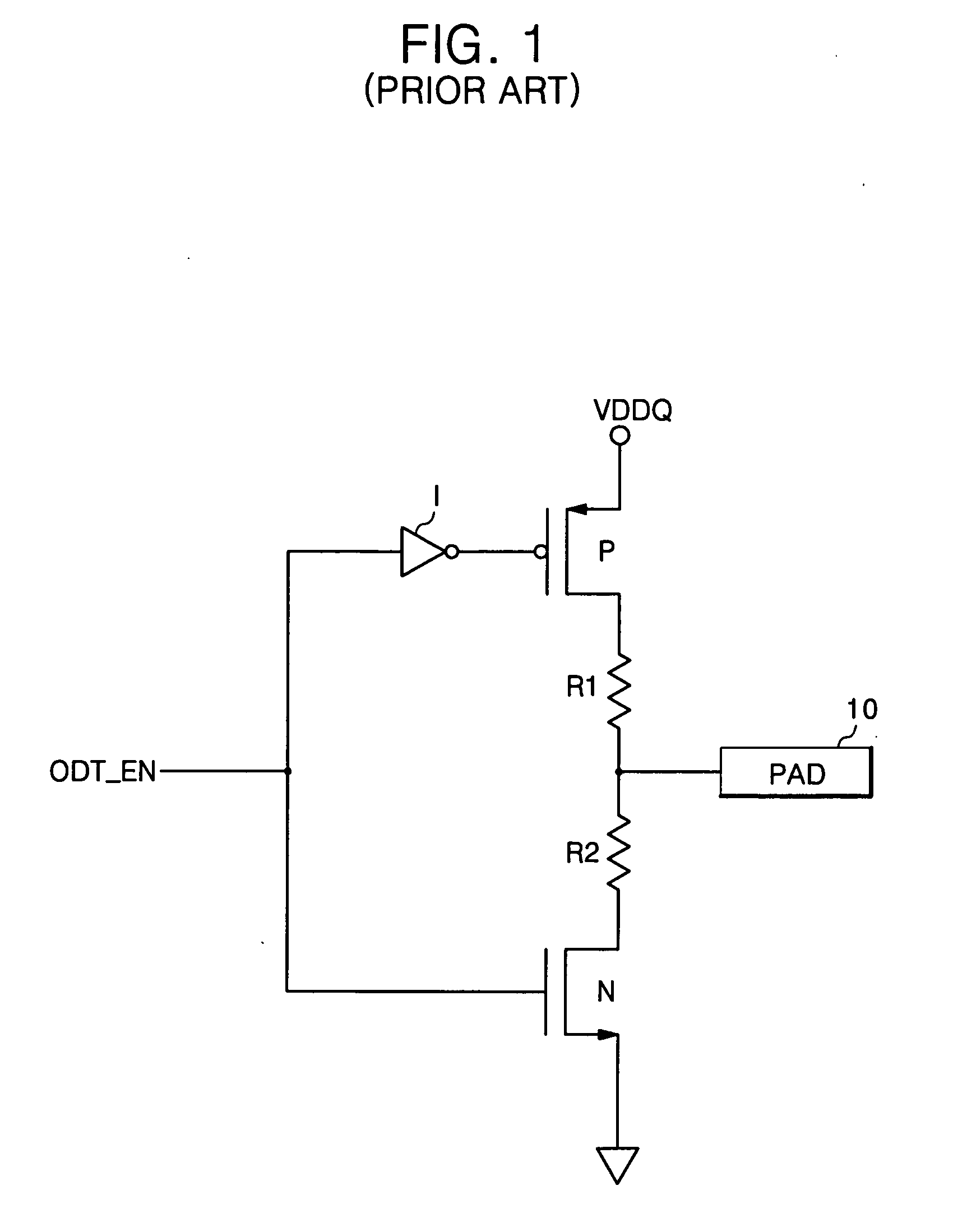
Accordingly, the on-die termination circuit of FIG. 1 has disadvantages associated with the capacitance of the PMOS transistor.
In addition, the electrical characteristics of the NMOS transistor and PMOS transistor may be different due to differences in the manufacturing process.

Method used


Image

  • Semiconductor integrated circuit device and on-die termination circuit
  • Semiconductor integrated circuit device and on-die termination circuit
  • Semiconductor integrated circuit device and on-die termination circuit

Examples


Embodiment Construction

[0021] The present invention will now be described more fully hereinafter with reference to the accompanying drawings, in which preferred embodiments of the invention are shown. This invention may, however, be embodied in different forms and the invention should not be construed as limited to the embodiments set forth herein.

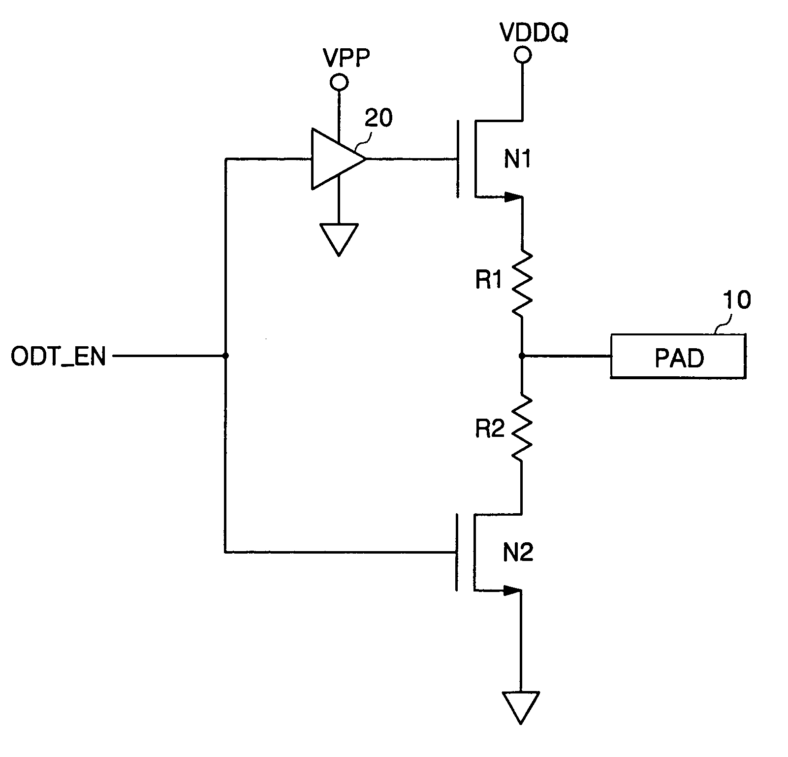
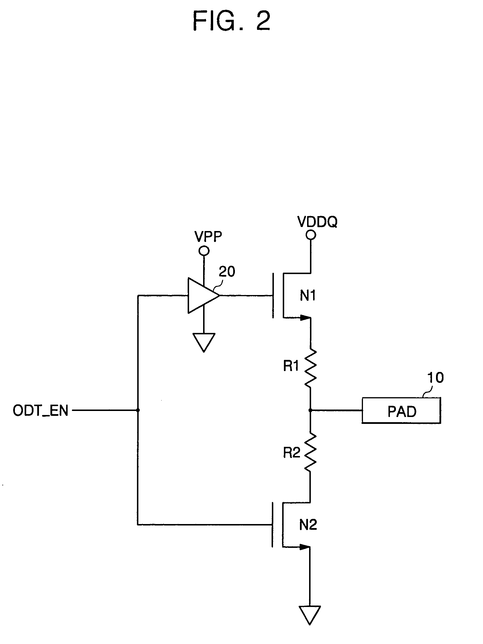
[0022]FIG. 2 is a circuit diagram illustrating an embodiment of the present invention. The circuit shown in FIG. 2 is an on-die termination circuit. The circuit includes a first NMOS transistor N1 connected to a power voltage VDDQ, a second NMOS transistor N2 connected to a ground voltage, a first termination resistor R1, a second termination resistor R2, and a level shifter 20.

[0023] The circuit shown in FIG. 2 performs substantially the same overall function as does the circuit shown in FIG. 1. However, the on-die termination circuit shown in FIG. 2 replaces the PMOS transistor P that is included in the circuit shown in FIG. 1 with the NMOS transistor N1. Ad...


PUM


Abstract

The present invention discloses a semiconductor integrated circuit device and an on-die termination circuit. The circuit includes a level shifter for boosting an on-die termination control signal to a high voltage level; and a first NMOS transistor connected between a power voltage and a pad and terminating the pad to a first termination voltage level in response to the high voltage level. The on-die termination circuit has a reduced input capacitance.

Description

CROSS-REFERENCE TO RELATED APPLICATION [0001] This application claims the benefit of Korean Patent Application No. 2004-21330, filed on Mar. 29, 2004. The entire disclosure of Korean Patent Application No. 2004-21330 is hereby incorporated herein by reference. BACKGROUND OF THE INVENTION [0002] 1. Field of the Invention [0003] The present invention relates to a semiconductor integrated circuit device and, more particularly, to an on-die termination circuit for a semiconductor integrated circuit device. [0004] 2. Description of the Related Art [0005] Lines used to transmit signals among different integrated circuit (IC) devices (e.g., microprocessor, memory controller, memory, etc) are often terminated by a termination circuit to prevent signals from being reflected. [0006] Signal reflection degrades signal integrity, and particularly as at higher system operating speeds, signal reflection can have a significant effect on signal integrity. In general, in order to prevent the maximum ...

Claims


Application Information

Patent Timeline
Patent Type & Authority Applications(United States)
IPC IPC(8): H03K19/003G11C7/10H03K19/0185
CPCH03K19/018528G11C5/147G11C7/1048G11C7/1051
Inventor CHUNG, IN-YOUNG
Owner SAMSUNG ELECTRONICS CO LTD
Learn More