Method for using a wet etch to manufacturing a semiconductor device having a silicided gate electrode and a method for manufacturing an integrated circuit including the same

a technology of gate electrode and manufacturing method, which is applied in the direction of semiconductor devices, electrical devices, transistors, etc., can solve the problems of poly doping affecting the work function the problem of silicided metal gates not being without problems, and the problem of polysilicon depletion becoming a serious issu

Active Publication Date: 2005-09-29
TEXAS INSTR INC
View PDF4 Cites 16 Cited by
  • Summary
  • Abstract
  • Description
  • Claims
  • Application Information

AI Technical Summary

Problems solved by technology

However, as device feature sizes continue to shrink, polysilicon depletion is becoming a serious issue.
Furthermore, poly doping has been shown to affect the work function of the silicided metal gates.
The silicided metal gates are not without their problems.
One of the more significant problems associated with the silicided metal gates is attributed to the simultaneous formation of the silicided metal gate and the silicided source / drain regions.
Deep silicided source / drain regions are nonetheless undesirable.
The main drawback of this approach originates from the across-wafer non-uniformity inherently associated with polishing (such as dishing, etc.).
As a result, the height of the poly gate after polishing may suffer significant variation.

Method used


Image

  • Method for using a wet etch to manufacturing a semiconductor device having a silicided gate electrode and a method for manufacturing an integrated circuit including the same
  • Method for using a wet etch to manufacturing a semiconductor device having a silicided gate electrode and a method for manufacturing an integrated circuit including the same
  • Method for using a wet etch to manufacturing a semiconductor device having a silicided gate electrode and a method for manufacturing an integrated circuit including the same

Examples


Embodiment Construction

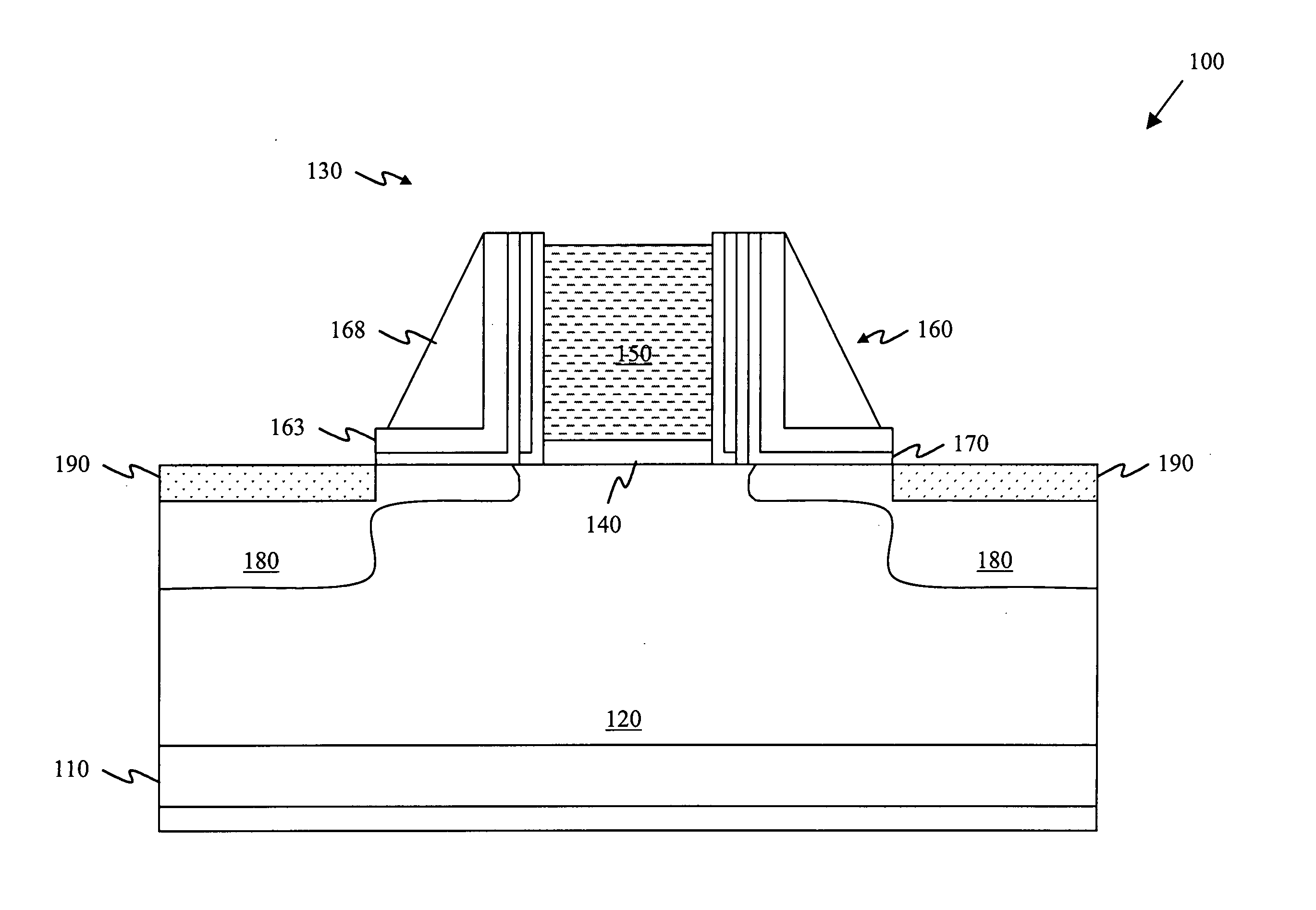
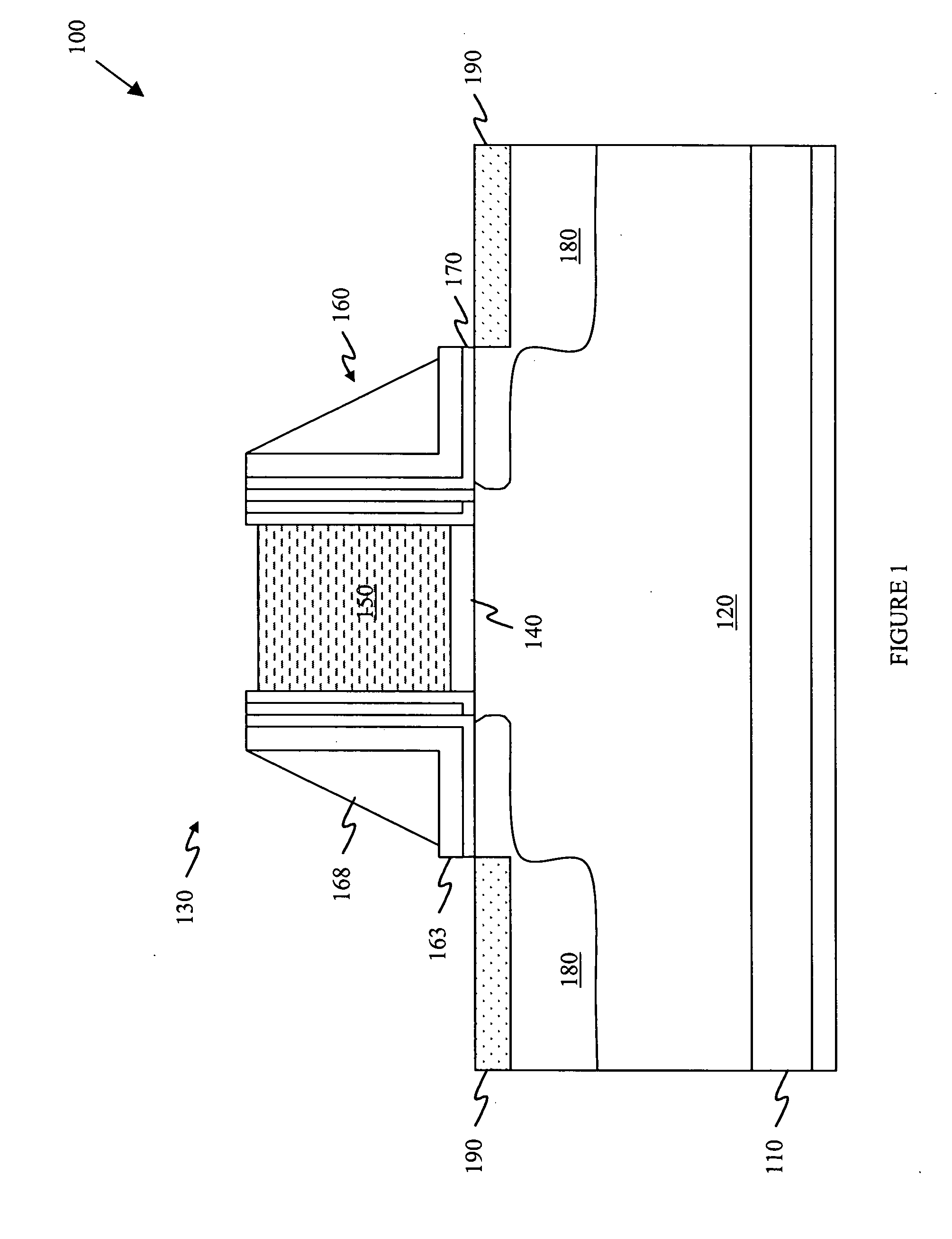
[0025] One inventive aspect of the present invention is the recognition that protective layers, particularly silicon nitride protective layers, may be used on the upper surface of an unsilicided polysilicon gate electrode to protect the unsilicided polysilicon gate electrode from many of the intermediate processes used in the manufacture of silicided metal gate electrode structures, as well as to control silicidation. In conjunction with this recognition is an equally important recognition that the thickness of the protective layer needs to be tailored such that it does not negatively affect the gate loop for both photo and etch, as well as allows the appropriate dopants therethrough to tailor the dopant profile of the completed silicided gate electrode. For this reason the thickness of the protective layer need not be too thick.

[0026] The present invention has recognized, however, that the optimum thickness for the protective layer, with regard to the gate loop for photo and etch,...


PUM


Abstract

The present invention provides a method for manufacturing a semiconductor device and a method for manufacturing an integrated circuit including the semiconductor device. The method for manufacturing the semiconductor device, among other possible steps, forming a polysilicon gate electrode (250) over a substrate (210) and forming a protective layer (260) over the polysilicon gate electrode (250) to provide a capped polysilicon gate electrode (230). The method further includes forming a protective oxide (510) on a surface proximate the polysilicon gate electrode (250), and removing the protective oxide (510) using a wet etch, the wet etch not having a substantial impact on the protective layer (260).

Description

CROSS-REFERENCE TO RELATED APPLICATIONS [0001] This application is a continuation-in-part of U.S. patent application Ser. No. 10 / 810,759, entitled “A METHOD FOR MANUFACTURING A SEMICONDUCTOR DEVICE HAVING A SILICIDED GATE ELECTRODE AND A METHOD FOR MANUFACTURING AN INTEGRATED CIRCUIT INCLUDING THE SAME, filed on Mar. 26, 2004. The above-listed application is commonly assigned with the present invention and is incorporated herein by reference as if reproduced herein in its entirety.TECHNICAL FIELD OF THE INVENTION [0002] The present invention is directed, in general, to a method for manufacturing a semiconductor device and, more specifically, to a method for using a wet etch to manufacture a semiconductor device having a silicided gate electrode and a method for manufacturing an integrated circuit including the same. BACKGROUND OF THE INVENTION [0003] Metal gate electrodes are currently being investigated to replace polysilicon gate electrodes in today's ever shrinking and changing t...

Claims


Application Information

Patent Timeline
Patent Type & Authority Applications(United States)
IPC IPC(8): H01L21/28H01L21/336H01L21/44H01L29/49H01L29/78
CPCH01L21/28097H01L29/4975H01L29/7833H01L29/6656H01L29/6659H01L29/66507H01L21/28052H01L21/28518
Inventor HALL, LINDSEYBU, HAOWENYU, SHAOFENG
Owner TEXAS INSTR INC
Why Eureka
Try Eureka