Quantum wire gate device and method of making same

a quantum wire gate and gate technology, applied in the field of integrated circuit fabrication, can solve the problems of increasing the length of the electron path, affecting the effective transition time, and unable to achieve the acceptable performance of 0.7 scaling,

Inactive Publication Date: 2005-09-29
INTEL CORP
View PDF9 Cites 44 Cited by
  • Summary
  • Abstract
  • Description
  • Claims
  • Application Information

AI Technical Summary

Problems solved by technology

During the tunneling of an electron from a source to a drain in a typical semiconductive transaction, an electron will suffer a number of collisions between source and drain that cause the electron path length to increase.
Because electron flow is constant velocity, the longer electron path hinders the effective transition time thereof.
The decrease in supply voltage, however, has caused acceptable performance in the 0.7× scaling to become increasingly elusive.

Method used


Image

  • Quantum wire gate device and method of making same
  • Quantum wire gate device and method of making same
  • Quantum wire gate device and method of making same

Examples


Embodiment Construction

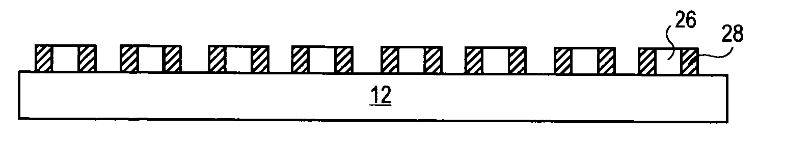
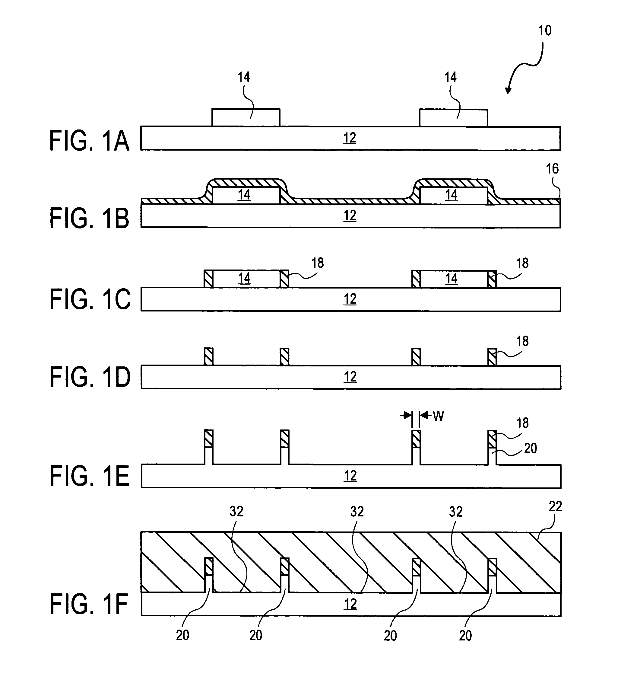
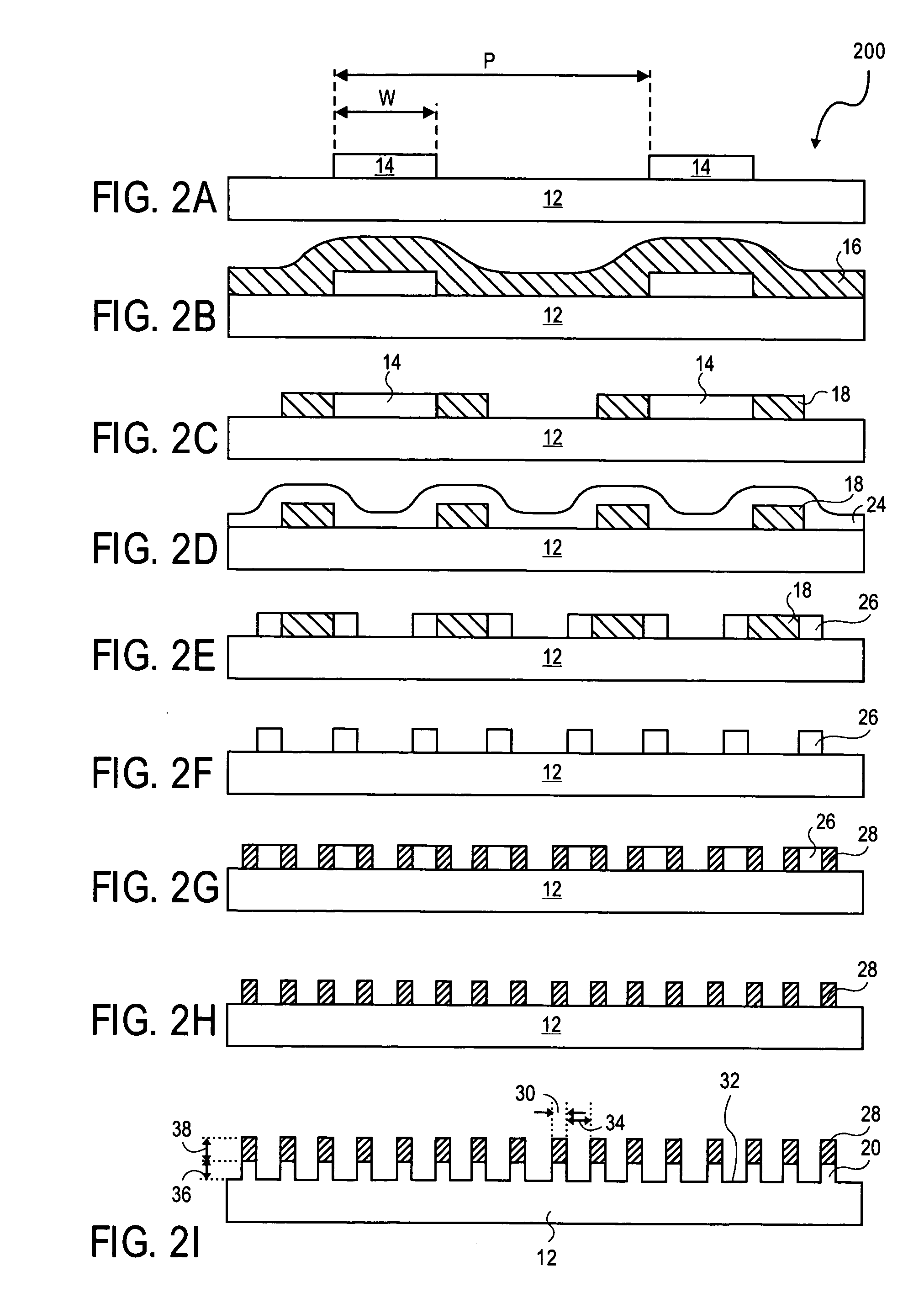
[0032] The following description includes terms, such as upper, lower, first, second, etc. that are used for descriptive purposes only and are not to be construed as limiting. The embodiments of an apparatus or article of the present invention described herein can be manufactured, used, or shipped in a number of positions and orientations.

[0033] Reference will now be made to the drawings wherein like structures will be provided with like reference designations. In order to show the structures of the present invention most clearly, the drawings included herein are diagrammatic representations of integrated circuit structures. Thus, the actual appearance of the fabricated structures, for example in a photomicrograph, may appear different while still incorporating the essential structures of the present invention. Moreover, the drawings show only the structures necessary to understand the present invention. Additional structures known in the art have not been included to maintain the ...


PUM

PropertyMeasurementUnit
pitchaaaaaaaaaa
pitchaaaaaaaaaa
widthaaaaaaaaaa

Abstract

The present invention relates to a method of forming a quantum wire gate device. The method includes patterning a first oxide upon a substrate. Preferably the first oxide pattern is precisely and uniformly spaced to maximize quantum wire numbers per unit area. The method continues by forming a first nitride spacer mask upon the first oxide and by forming a first oxide spacer mask upon the first nitride spacer mask. Thereafter, the method continues by forming a second nitride spacer mask upon the first oxide spacer mask and by forming a plurality of channels in the substrate that are aligned to the second nitride spacer mask. A dielectric is formed upon the channel length and the method continues by forming a gate layer over the plurality of channels. Because of the inventive method and the starting scale, each of the plurality of channels is narrower than the mean free path of semiconductive electron flow therein.

Description

BACKGROUND OF THE INVENTION [0001] 1. Field of the Invention [0002] The present invention relates generally to integrated circuit fabrication, and, more specifically, the present invention relates to the fabrication of quantum wire gate structures that are spacer-width patterned. [0003] 2. Description of Related Art [0004] During the tunneling of an electron from a source to a drain in a typical semiconductive transaction, an electron will suffer a number of collisions between source and drain that cause the electron path length to increase. Because electron flow is constant velocity, the longer electron path hinders the effective transition time thereof. With the advent of quantum wire devices, an electron is allowed only to suffer collisions that will be confined within the extremely narrow channel, including collisions at the interface between channel and contiguous dielectric. Thus, where the narrow channel has a width the is less than the mean free path (MFP) of the electron, c...

Claims


Application Information

Patent Timeline
Patent Type & Authority Applications(United States)
IPC IPC(8): H01L21/308H01L21/335H01L21/336H01L21/8234H01L29/775H01L29/786
CPCB82Y10/00H01L21/3086H01L21/3088H01L21/823412Y10S438/962H01L29/66439H01L29/66795H01L29/775H01L29/785H01L21/823437
Inventor DOYLE, BRIAN
Owner INTEL CORP
Why Eureka
Try Eureka