Edge-triggered master + LSSD slave binary latch

a binary latch and master technology, applied in the field of new binary latches, can solve the problems of skew-managed three lssd testclock trees, complex test logic of circuits containing these latches, etc., and achieve the effect of higher driving capabilities

Inactive Publication Date: 2005-09-29
IBM CORP
View PDF5 Cites 21 Cited by
  • Summary
  • Abstract
  • Description
  • Claims
  • Application Information

AI Technical Summary

Benefits of technology

[0009] An embodiment of this invention provides a binary latch with an edge-triggered master flip-flop, with a clock input connected to the system clock, with a data input and with an output, said output is connected to a level sensitive scan design (LSSD) slave latch. This combination is novel and easy to use in LSSD testing with the NAND gate with a first input connected to the system clock, a second input connected with a test input and with an output connected to the LSSD slave latch clock input.
[0012] An amplifier element can be connected to the output of the LSSD slave latch to provide higher driving capabilities to the output of the binary latch.

Problems solved by technology

They have the disadvantage that testing the logic of a circuit containing these latches is rather complex and has to be performed with functional vectors provided by the chip designer.
The three LSSD testclock trees are mostly not well skew-managed, which makes it often necessary to apply the tests with a lower frequency.

Method used


Image

  • Edge-triggered master + LSSD slave binary latch
  • Edge-triggered master + LSSD slave binary latch
  • Edge-triggered master + LSSD slave binary latch

Examples


Embodiment Construction

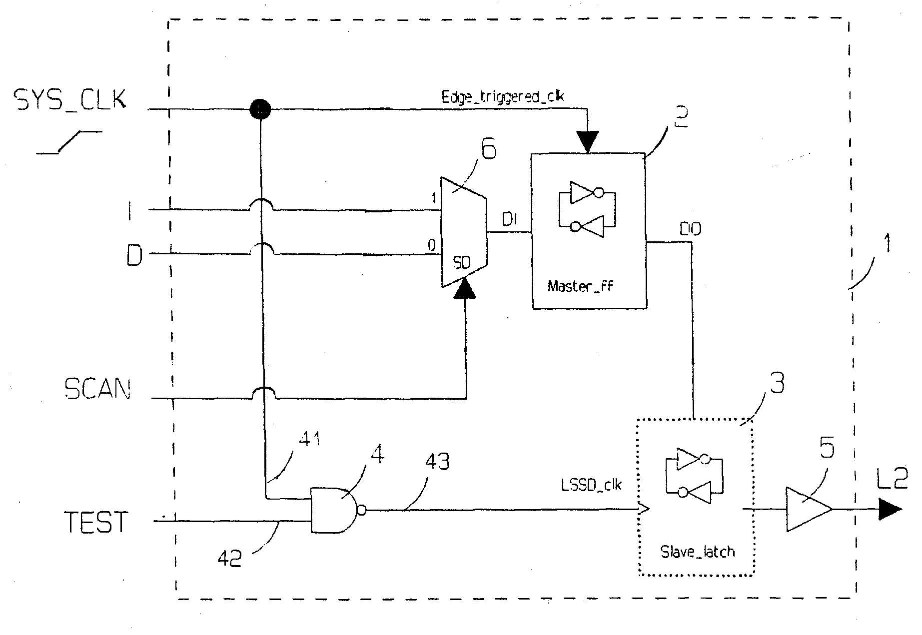
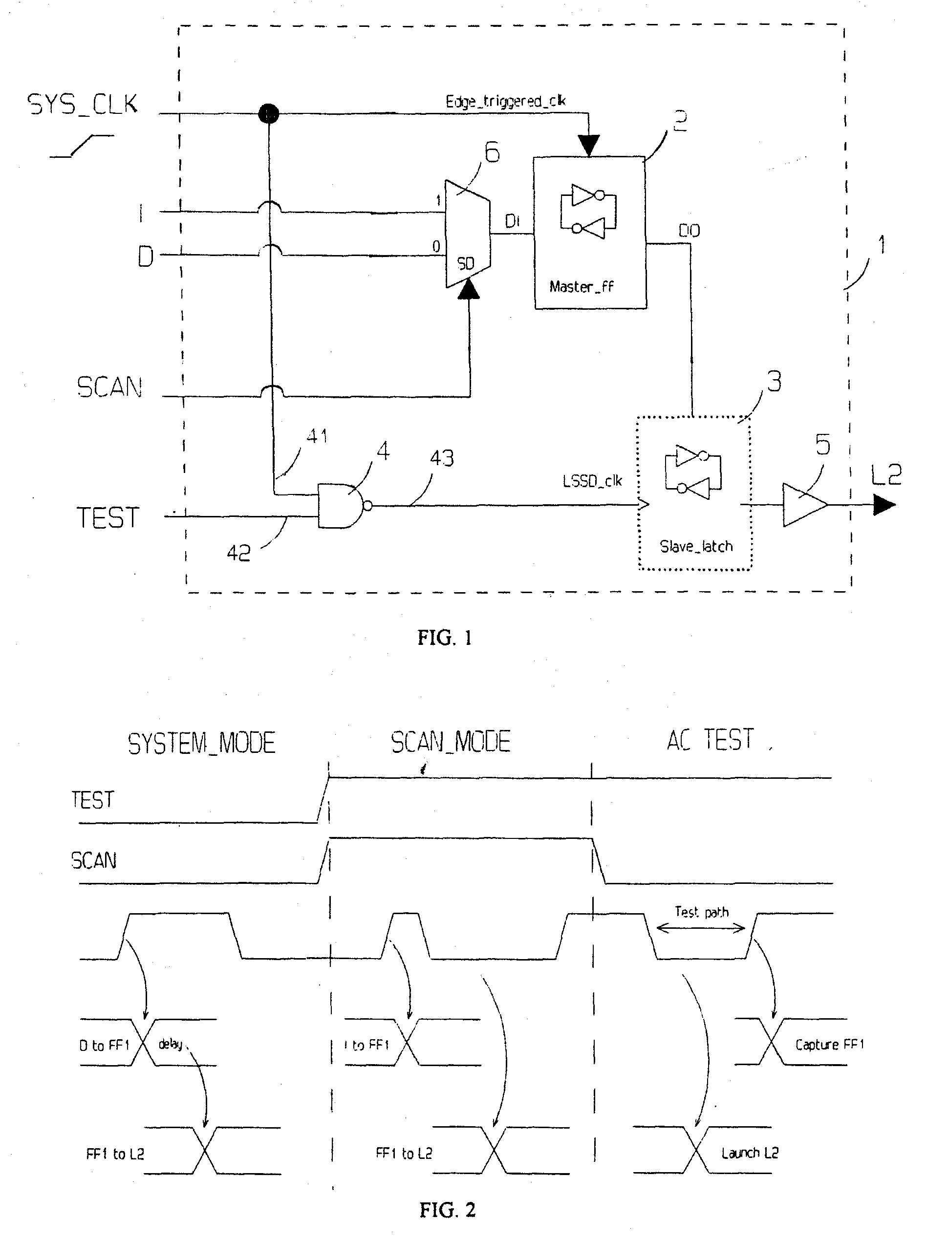
[0018]FIG. 1 depicts a binary latch 1 with an edge triggered master flip-flop 2, with a clock input (edge-triggered clock input) connected to the system clock SYS_CLK. The master flip-flop 2 has a data input DI, which is connected to the output of a multiplexer 6, which connects data signals D or scan input signals I according to a selection signal SCAN with the master flip-flop.

[0019] The output DO of master flip-flop 2 is connected to a level sensitive scan design (LSSD) slave latch 3. This novel combination allows testing the device with LSSD principals, yet have the circuit behave in functional mode as an edge-triggered flip-flop.

[0020] The clock signals for the slave latch are provided by a NAND gate 4 with a first input 41 which is connected to the system clock SYS_CLK and a second input 42 which is connected with a test input TEST.

[0021] The output 43 of the NAND gate 4 is connected to the LSSD slave latch clock input LSSD_clk.

[0022] This makes the LSSD slave latch 3 beha...


PUM


Abstract

Disclosed is a binary latch that operates as an edge-triggered flip-flop and which is LSSD-testable. The binary latch comprises an edge triggered master flip-flop (2), with a clock input connected to the system clock (SYS_CLK), with a data input (DI) and with an output (DO), a level sensitive scan design (LSSD) slave latch (3), connected to the output (DO) of the master flip-flop (2), a NAND gate (4) with a first input (41) connected to the system clock (SYS_CLK), a second input (42) connected to a test input (TEST) and with an output (43) connected to the LSSD slave latch clock input (LSSD_clk).

Description

BACKGROUND OF THE INVENTION [0001] 1. Field of the Invention [0002] The present invention relates to a novel binary latch comprising a master flip-flop and a slave latch. [0003] 2. Description of Related Art [0004] Binary latches are commonly built up with edge-triggered elements; examples are master-only or master and slave flip-flop circuits. Such binary latches have been used in chip architecture for a long time and are present in large quantities for example in registers or state machine design. They have the disadvantage that testing the logic of a circuit containing these latches is rather complex and has to be performed with functional vectors provided by the chip designer. [0005] Another common way to build latches is based on the level sensitive scan design (LSSD) known in the state of the art, which allows testing in an easier way. Such binary latches combine an LSSD master and LSSD slave to a shift register latch pair (SRL). In order to make an LSSD latch perform like an ...

Claims


Application Information

Patent Timeline
Patent Type & Authority Applications(United States)
IPC IPC(8): G01R31/28G01R31/3185G11C29/00H03K3/037
CPCG01R31/318541H03K3/0375G11C29/003
Inventor VERWEGEN, PETER
Owner IBM CORP
Why Eureka
Try Eureka