Semiconductor device

a technology of semiconductor devices and semiconductors, applied in semiconductor devices, semiconductor/solid-state device details, electrical apparatus, etc., can solve the problems of obstructing the reduction of packaging cost and high cost of mounting substrates, and achieve the effect of improving heat dissipation performance and reducing packaging cos

Inactive Publication Date: 2005-10-06
RENESAS ELECTRONICS CORP
View PDF5 Cites 41 Cited by
  • Summary
  • Abstract
  • Description
  • Claims
  • Application Information

AI Technical Summary

Benefits of technology

[0010] The present inventors have made studies about improving the heat dissipating performance of a high output semiconductor device having a sealing body formed of an insulating resin and also about reducing the packaging cost.

Problems solved by technology

As a result, the cost of the mounting substrate becomes high, obstructing the reduction of the packaging cost.

Method used


Image

  • Semiconductor device
  • Semiconductor device
  • Semiconductor device

Examples


first embodiment

[0072] FIGS. 1 to 12 are related to the structure of a semiconductor device according to a first embodiment of the present invention. FIGS. 13 to 23 are related to a method of manufacturing the semiconductor device of the first embodiment. FIGS. 24 to 30 are related to a semiconductor device package structure as part of an electronic device in which the semiconductor device of the first embodiment is incorporated.

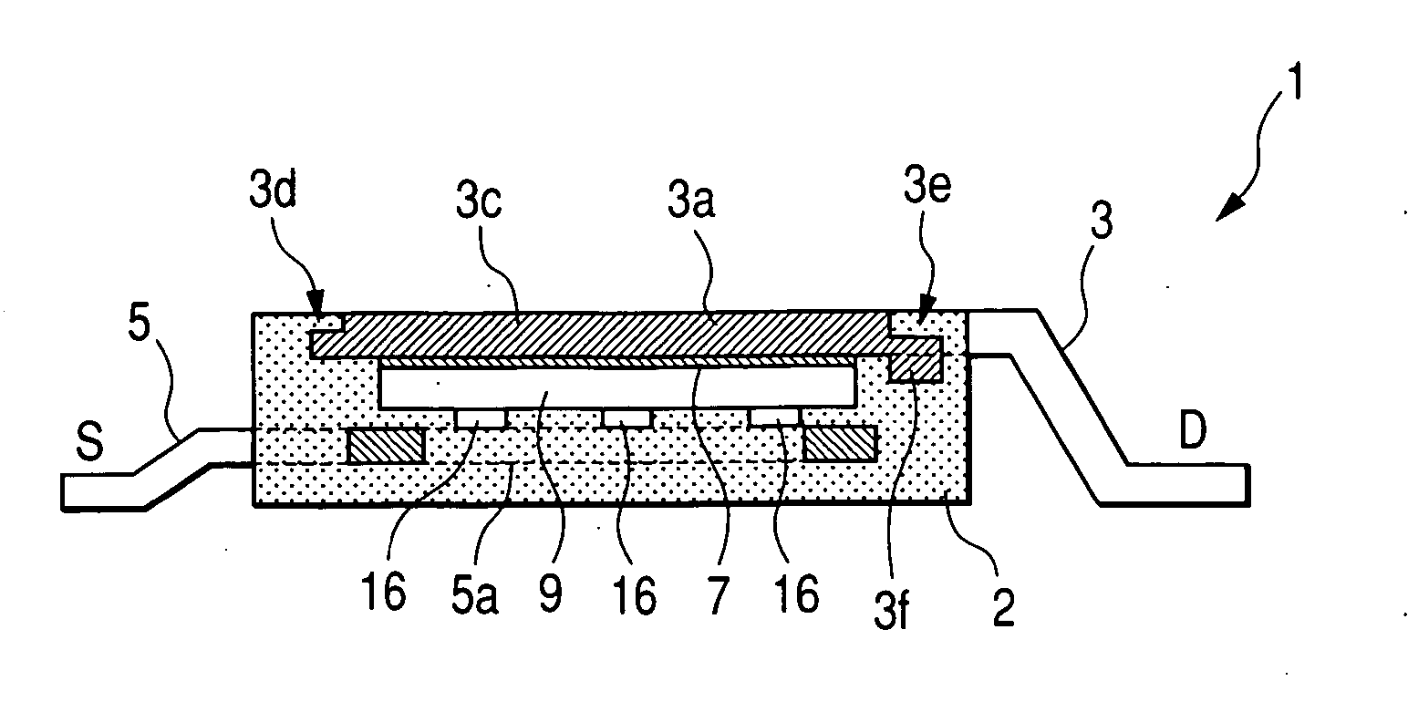
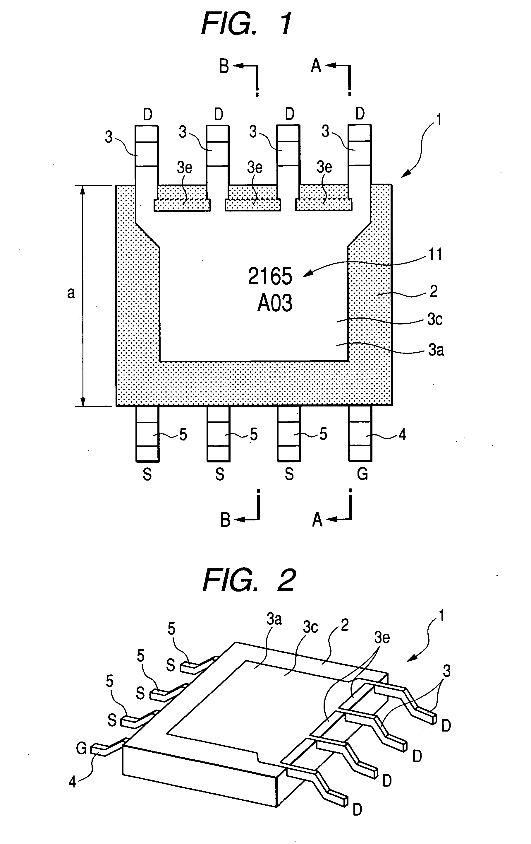
[0073] In this first embodiment, reference will be made to an example in which the present invention is applied to a power MOSFET device (semiconductor device). In the power MOSFET device is incorporated a semiconductor chip formed with a vertical power MOSFET. A source (S) electrode as a first electrode and a gate (G) electrode as a control electrode are provided on a first main surface of the semiconductor chip, while a drain (D) electrode as a second electrode is provided on a second main surface opposite to the first main surface. The second electrode serves as a back ...


PUM


Abstract

A semiconductor device superior in heat dissipating performance and permitting reduction of the packaging cost is provided. The semiconductor device comprises a sealing body formed of an insulating resin, a semiconductor chip positioned within the sealing body, the semiconductor chip having a gate electrode and a source electrode on a first main surface thereof and having a back electrode (drain electrode) on a second main surface thereof, a drain electrode plate projecting in a gull wing shape on one end side of the sealing body, an upper surface of a portion of the drain electrode plate which portion is positioned in the sealing body being exposed from the sealing body and a lower surface thereof being connected to the back electrode through an adhesive, a gate electrode plate projecting in a gull wing shape on an opposite end side of the sealing body and being connected to the gate electrode within the sealing body, a source electrode plate projecting in a gull wing shape on the opposite end side of the sealing body and being connected to the source electrode within the sealing body, a depression formed in the surface of the drain electrode plate within the sealing body and filled with the resin which forms the sealing body, and a projecting portion formed on the surface of the drain electrode plate within the sealing body and engaged with the sealing body. The drain electrode plate and the source electrode plate branch into plural branch pieces (leads) serving as gull wing-shaped surface mounting terminals.

Description

CROSS-REFERENCE TO RELATED APPLICATION [0001] The present application claims priority from Japanese patent application No. 2004-065413 filed on Mar. 9, 2004, the content of which is hereby incorporated by reference into this application. BACKGROUND OF THE INVENTION [0002] The present invention relates to a semiconductor device and a method of manufacturing the same. Particularly, the present invention is concerned with a technique applicable effectively to the manufacture of a semiconductor device wherein a semiconductor chip which generates a large amount of heat is sealed. [0003] As a high output semiconductor device there is known a semiconductor device wherein a semiconductor chip formed with a power transistor is incorporated within a sealing body. As examples of power transistors are mentioned power MOSFET (Metal Oxide Semiconductor Field-Effect-Transistor), IGBT (Insulated Gate Bipolar Transistor), and bipolar power transistor. [0004] A power MOSFET device is of a structure w...

Claims


Application Information

Patent Timeline
Patent Type & Authority Applications(United States)
IPC IPC(8): H01L23/495H01L23/29
CPCH01L23/49562H01L2924/01033H01L2224/1134H01L2224/131H01L2224/13144H01L2224/32245H01L2924/01005H01L2924/01013H01L2924/01015H01L2924/01029H01L2924/01047H01L2924/01079H01L2924/01082H01L2924/13055H01L2924/13091H01L2924/14H01L2924/1433H01L2924/1305H01L2924/1306H01L2224/73253H01L2224/16245H01L2924/00013H01L2924/01006H01L24/33H01L2924/014H01L2924/00014H01L2224/13099H01L2924/3512H01L2924/00H01L2924/181H01L2924/12042H01L2924/00012
Inventor HATA, TOSHIYUKIOTANI, TAKESHISHIMIZU, ICHIO
Owner RENESAS ELECTRONICS CORP
Why Eureka
Try Eureka